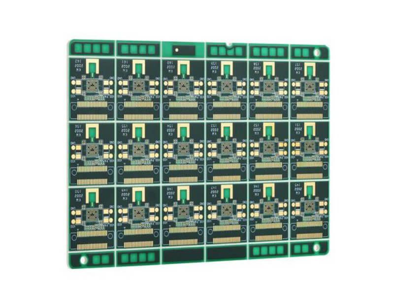
Fabrication Datums and Fiducials in PCB Design
Every process in PCB manufacture locates the work against something. Drilling, imaging, pressing and placement all have to know where the board is before they can act on it, and they all get that answer from datums that the designer placed in the layout. When those datums are missing, badly placed or inconsistent, the result is not a clean failure but a slow accumulation of positional error that shows up later as layers that do not align, holes that miss their lands or components placed slightly off their pads.
What a Fabrication Datum Does
A datum is a defined point, line or surface that the rest of the work is measured from. In PCB manufacturing it performs three jobs.
It locates the panel on the machine, so that the tool acts where the design intends rather than where the operator happened to place the board. It aligns the layers of a multilayer stack, so that the pattern on one layer lands on the pattern of the layers already bonded. And it provides a common reference for measurement, so that a dimension checked on the finished board means the same thing as the dimension in the drawing.
All three jobs are about agreement. The datum is the coordinate origin the design, the fabricator and the assembly house all work from, and if any of the three is working from a different origin, the difference appears as a defect.
Three Levels of Datum
Datums in a typical design work at three levels of scope, and each answers a different question.
Global origin. The overall reference for the panel, usually placed at a corner or within the process border rather than inside the area that carries circuitry. It is what the drill programme, the imaging equipment and the press tooling all reference, and it is what keeps the finished outline dimensionally correct.
Local origin. A reference established for a specific high-density area, typically around a fine-pitch package, used to correct position locally rather than assuming that a correction applied to the panel also applies to the middle of it. On large panels, small errors at the edges grow into larger ones further in, and a local reference is how that growth is compensated.
Fiducials. Round marks that assembly equipment recognises optically, used by pick and place machines to establish the position of the panel and of individual circuits, and by inspection systems to register their images. They are copper features with the solder mask opened over them, so that the machine sees a solid, high-contrast shape.
Fiducial Geometry and Clearance
A fiducial that cannot be recognised reliably is worse than none, because it produces intermittent misplacement rather than a consistent error that can be corrected.
The mark itself is a filled copper shape, normally circular, with a defined diameter and a solder mask opening slightly larger so that the mask does not encroach on the edge. Around it, the design has to leave a clear area free of copper, traces, mask features and silkscreen, wide enough that the vision system sees the mark against a uniform background rather than against pattern.
Three of them are normally placed per panel or per circuit for the placement equipment, arranged so that they are not collinear, because three points define position and rotation while two define only a line. Assembly fiducials are usually smaller than the machine datum features used earlier in fabrication, since the vision systems that read them are optical and resolution-limited rather than mechanical.
Setting Datums Well
The principles are short and each of them has a failure mode behind it.
Datums must be visible. A mark under solder mask, under silkscreen or under a component is not a datum. Marks must sit where the process will not damage them, which rules out the extreme edge of the panel where handling and routing act. They must be stable, which means avoiding areas near large copper planes that move during pressing or near the outline where material is removed. They must be numerous enough: a multilayer board needs a reference on each layer that has to align with the others, and the panel needs references for the processes that work on the whole panel as well as those that work on the individual circuit.
They must also follow the standard the industry uses, so that the equipment that reads them sees a shape and a size it recognises. A datum that is individually reasonable but outside the convention costs the fabricator time and the designer a query.
Finally, datums have to be considered together with the process border. That border, and any tooling features placed in it, are what the equipment grips and references. Layout decisions inside the circuit area cannot be made as though the border did not exist, because the two are part of the same coordinate system.

What Goes Wrong Without Them
The failures are recognisable, and each maps to the datum that was missing.
Layer misalignment, where a hole lands off the centre of its land or an inner layer pattern is offset from the outer, is a failure of layer-to-layer agreement and points at the alignment references used in pressing and drilling. Holes drilled in the right place relative to the panel but the wrong place relative to the circuitry point at a global reference that does not match the one the artwork was generated from. Components placed consistently offset, or offset by a different amount on each circuit, points at assembly fiducials that are missing, too few or unrecognisable. And a dimensional error that grows from one end of the panel to the other suggests a global reference that is too far from the area it is supposed to locate.
None of these are caught by a functional test on a single board. They appear as yield loss across a batch, which is why the datum design is part of the layout review rather than an afterthought.
Datums, Panelisation and Tooling
Datums are difficult to discuss separately from panel design, because the panel is where they operate. The way circuits are arranged on the panel, the width of the border, the position of tooling holes and the routing or scoring method all determine whether the references remain usable through the whole process.
A useful test is to follow a reference through the sequence. If a datum exists on a layer but disappears after lamination, if a fiducial is placed where the router will remove it, or if a tooling hole is used for a process that then changes its position, the design will produce boards that are correct in theory and inconsistent in practice.
Where Design and Fabrication Meet
The design choices that make fabrication predictable are not advanced: a border of adequate width for tooling, references that survive every process, clear areas around the marks that the equipment reads, and a panel layout that keeps the circuit area separate from the features that exist to serve the process. Each of them costs a small amount of board area and each of them prevents a class of defect that is expensive to diagnose after the fact.
Reviewing them belongs with the rest of the manufacturability checks before the files are released. Our DFM review describes how that review runs, and the layout quality checklist lists the items that should be signed off, including the placement of the references the machines depend on.

FAQ
How many fiducials does a panel need? At least three per panel or per circuit for the placement equipment, placed so they are not in a straight line, in addition to the references the fabrication processes use.
Can a fiducial be covered by solder mask? No. Covering the mark removes the contrast the vision system needs and makes the result unreliable rather than simply degraded.
Why do large panels need local references? Because positional error accumulates across the panel. A correction measured at the edge does not describe the centre, so a local reference is used where fine pitch requires tighter agreement.