Flying Probe PCBA Testing: System and Process Guide
Flying probe PCBA testing is an electrical test method that moves small probes to each test point instead of using a fixed bed-of-nails fixture. It is an improvement of the online needle bed tester and is especially useful for prototypes, low-volume boards, and high-density assemblies where a dedicated fixture is not practical.
The flying probe tester uses two or more sets of probes that can move within a specific test area. The probes are driven by motors and contact the test points according to a programmed coordinate sequence.
This guide explains the basic composition and working principle of a flying probe test system used in SMT processing.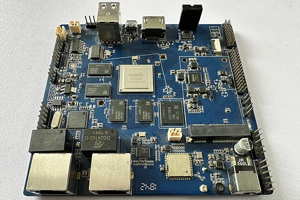
How Flying Probe Testing Works
A flying probe tester replaces the non-movable needle bed with moving probes. A mobile probe driving structure is added to the system, and motors move the probes in the horizontal and vertical directions.
The horizontal positioning mechanism moves the probe above the correct test point, and the vertical mechanism lowers the probe into contact. The test can then be performed on the component or connection.
Each test probe performs open-circuit, short-circuit, or component tests according to the test procedure. The probes move from one test point to the next without a physical fixture.
A flying probe tester usually has eight test probes, four test heads, and a minimum test clearance of about 0.2 millimeters.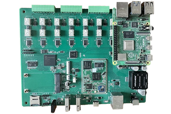
Advantages Over Bed-of-Nails Test
Bed-of-nails testing uses a fixed fixture with pins that contact the board test points. Building a fixture takes time and is expensive for a small number of boards.
Flying probe testing does not need a special fixture. The probe coordinates are programmed from the board data, so a new product can be tested more quickly.
This makes the flying probe tester ideal for prototypes, fast-turn boards, and design changes. It can also test boards with high component density where there is no room for a full fixture.
The trade-off is that flying probe testing is slower than bed-of-nails testing because each probe must move to every test point.
Component 1: Computer System
The flying probe tester uses a computer system to control the test process. The system is usually equipped with special instrument cards, video cards, and driver cards for the PC-based test system.
If the system has higher functional requirements, a network hub or workstation system can be used.
The test software defines the probe movement sequence, measurement functions, and pass or fail limits. The interface should be clear so that operators can start the test and read the result easily.
Newer systems use modern operating systems and graphical software, while some older systems use a simpler command interface.
Component 2: Instrument and Measurement Module
Most instruments and measurement modules are located at the bottom of the flying probe test system. They provide the test excitation signals and the measurement devices.
The system can include a programmable DC voltage and current source, a multifunction waveform generator for sine, triangle, and square waves, a clock generator, a voltmeter, a counter, and pull-up or pull-down resistors.
These instruments let the tester check component values, semiconductor behavior, and open or short circuits.
A switch system is integrated into the instrument interface card. The test program can connect different instruments to the probe and board automatically.
Component 3: Motion and Drive System
Flying probe movement can be divided into horizontal and vertical motion. The horizontal XY drive moves the probe within the working area to find and locate the test points.
When the screw drive system moves, the drive arm travels to the correct coordinate. Digital cameras are often used to find the test point before the probe makes contact.
Vertical motion has one purpose: to bring the probe into contact with the test point. The probe usually touches at a small inclination angle of about 5 degrees from the vertical.
The probe motion system must have fast and high-precision positioning ability to reduce test time while maintaining accuracy.
Drives for the Probe System
The probe support arm and probe are driven by motors. The Y axis is often driven by a brushless motor and a precision lead screw with an integrated encoder.
Some manufacturers use advanced drive technologies such as air bearings and linear motors for even higher speed and accuracy.
The Z axis of the probe is usually driven by a linear motor or a precision stepping motor. The drive must control the contact force so the probe does not damage the pad or component.
Correct drive selection reduces vibration, improves repeatability, and allows smaller test points to be contacted reliably.
Component 4: Test Area
The test area of the flying probe system is usually located near an operation panel. It contains the mechanical positioning device for the board under test.
The bottom of the test area is often used to expand the testing capability. Auxiliary access devices can be added to connect power, test excitation signals, and non-vector test equipment.
The test area should have a protective cover to protect the safety of the operator while the probes are moving.
The board holder must align the board repeatably so that every test program finds the test points at the correct position.
Program and Probe Selection
The flying probe is selected according to the actual test need and the shape of the test point. A sharp probe is used for small pads, while a wider probe may be needed for larger test points.
The engineer should also consider the height of probe movement, the movement angle to the test point, the direction of movement, the impact force, and the search method.
These details affect test time, reliability, and the life of the probe and pad.
The program should include the safe approach path so that the probe does not hit a tall component or connector while moving.
Handling Component Height Differences
Assembled circuit modules have components with different heights. The probe must rise above tall components and then lower to the correct height before contacting a test point.
The programmer should consider component heights when the test program is created. This information is often not given accurately in the circuit design file, so it must be measured or extracted from the assembly data.
If the probe collides with a tall component, the component or the probe can be damaged. Clearance checks should be part of the test program verification.
Advanced systems may use a height map of the board to plan the probe path automatically.
Flying Probe Test Coverage
A flying probe tester can check opens, shorts, resistance, capacitance, diode direction, and many other electrical conditions. The test coverage depends on the available test points and the test program.
Boards without test points cannot be tested effectively by flying probe. The PCB layout should include test points whenever ICT or flying probe testing is planned.
Flying probe testing is slower than fixture-based testing, so it is most suitable for lower volume or when fixture cost is not justified.
For high-volume products, a bed-of-nails tester is faster, while flying probe can be used for new product bring-up and field returns.
A professional PCBA testing service should choose between flying probe, ICT, and functional test based on the board design and volume.
The test strategy should be discussed during PCB design and layout so that the board includes enough test points and clearance for the probes.
Flying probe testing can be combined with SMT PCB assembly and AOI to catch both visible and electrical defects before the board reaches functional test.
Test records should be managed through quality management so that every tested board has a complete history.
Test Point Design Rules
Flying probe test points should be placed on the outer layers of the board. A test pad of at least 0.5 millimeters is usually recommended, with enough clearance for the probe tip. The designer should also leave space around the pad so the probe can approach without touching solder mask or another component.
Test points should be connected directly to the net and should not be isolated by a series resistor unless the test plan requires it. Every important power, ground, and signal net should have at least one accessible test point.
The board assembly drawing should identify the test point locations. This helps the test engineer create the program and helps the operator repair a board when a fault is reported.
Reading and Recording Test Results
The flying probe software should display each failed test with the probe coordinate and the measured value. The report should compare the measured value with the limit and identify whether the failure is an open, short, resistance error, or diode fault.
When a board fails, the operator should follow the repair procedure and retest after the repair. The failure data should be summarized to show which test points or component values fail most often.
A repeated failure in the same net usually indicates a manufacturing problem such as a broken trace, a poor via, or a wrong component. The engineer can use the report to focus the inspection on the correct board area.
Conclusion
Flying probe PCBA testing uses moving probes to check opens, shorts, and component values without a fixed fixture. It is flexible and fast to set up for prototypes and low-volume boards.
The system includes a computer, instrument modules, a precision motion system, and a protected test area. Program planning must account for component height and probe movement.
When combined with other inspection methods, flying probe testing gives reliable electrical verification for high-density SMT assemblies.