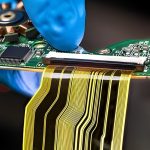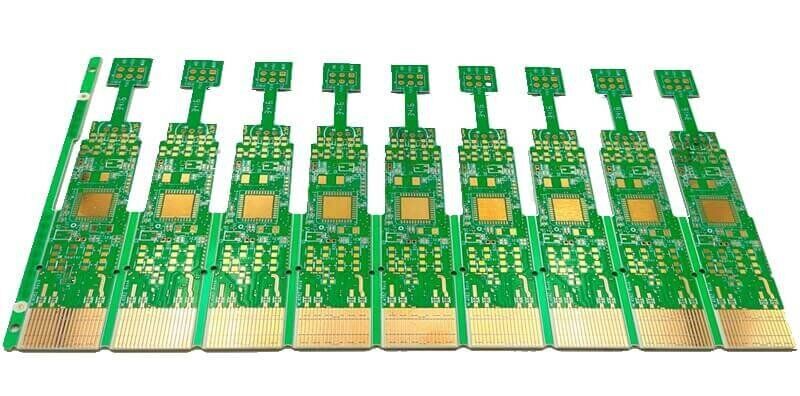
Electronic devices often require reliable interfaces between circuit boards and external connectors. When a PCB needs to be inserted into a connector repeatedly, the contact area must provide stable electrical conductivity, mechanical durability, and resistance to wear and oxidation. This is where Gold Finger PCB technology becomes particularly important.
A Gold Finger PCB is a printed circuit board with a series of exposed conductive contacts along one or more board edges. These contacts are typically finished with hard gold and are designed to mate with a corresponding connector.
Because the contact pads resemble a row of fingers, they are commonly called PCB Gold Fingers.
Gold fingers are widely used in expansion cards, memory modules, computer interfaces, industrial control boards, communication equipment, and other applications that require repeated insertion and removal.
Unlike conventional ENIG surface finishing, gold fingers are generally designed specifically for mechanical contact and therefore require a harder and more wear-resistant gold plating structure.
What Are PCB Gold Fingers?
PCB Gold Fingers are exposed copper contacts located along the edge of a printed circuit board. During operation, these contacts slide into a mating connector to establish an electrical connection between the PCB and another circuit or system.
A typical gold finger consists of:
- Copper conductor
- Nickel barrier layer
- Hard gold surface layer
The nickel layer provides a barrier between the copper and gold while contributing to mechanical durability. The hard gold layer protects the contact surface against oxidation, corrosion, and repeated mechanical wear.
The gold fingers are normally designed with carefully controlled dimensions, spacing, bevel angle, plating thickness, and surface quality to ensure reliable insertion into the connector.
Why Is Hard Gold Used for PCB Gold Fingers?
The main reason for using Hard Gold Plating on edge contacts is mechanical durability.
Although gold itself provides excellent corrosion resistance and electrical stability, pure or soft gold is not always suitable for repeated mechanical contact. Gold fingers therefore commonly use a harder gold alloy or a hard-gold plating system designed for connector applications.
Key benefits include:
- Excellent resistance to oxidation
- Good electrical conductivity
- High corrosion resistance
- Good resistance to mechanical wear
- Reliable repeated mating
- Stable contact performance
- Long service life
These properties make hard gold particularly suitable for boards that are inserted and removed frequently.
Examples include memory modules, expansion cards, industrial control boards, and communication interface boards.
Gold Finger PCB vs. ENIG PCB
Gold fingers are sometimes confused with ENIG, but the two finishes serve different purposes.
ENIG PCB uses an electroless nickel layer covered by a thin immersion gold layer. It is widely used for component pads because it provides a flat, solderable surface.
Gold fingers, on the other hand, are primarily intended for mechanical and electrical contact.
| Feature | Gold Finger PCB | ENIG PCB |
|---|---|---|
| Primary purpose | Repeated electrical contact | Component soldering |
| Typical location | PCB edge | Component pads |
| Mechanical wear resistance | High | Not intended for repeated sliding contact |
| Gold type | Typically hard gold | Immersion gold |
| Typical application | Edge connectors | SMT and component assembly |
| Beveled edge | Common | Generally not required |
Therefore, ENIG should not simply be treated as a substitute for gold fingers when a PCB will experience repeated insertion and removal.
Types of PCB Gold Fingers
Gold finger structures can be categorized according to the shape, length, and arrangement of the edge contacts.
1. Standard Gold Fingers
Standard gold fingers consist of regularly arranged rectangular contact pads along the PCB edge.
The contacts normally have similar widths, spacing, and lengths.
This is one of the most common configurations and is widely used in:
- Memory modules
- Expansion cards
- Interface boards
- Industrial control cards
- Communication equipment
The contact dimensions must match the corresponding connector to ensure reliable electrical and mechanical engagement.
2. Segmented Gold Fingers
Segmented gold fingers have contact pads that are intentionally separated or arranged with different lengths along the board edge.
The segmentation can be used to meet specific connector or electrical sequencing requirements.
For example, some contacts may engage before others during insertion. This can support functions such as grounding or controlled power sequencing, depending on the system design.
3. Different-Length Gold Fingers
Some Gold Finger PCB designs use contacts with different lengths.
This configuration can be used to control the order in which individual electrical connections are established when the board is inserted into a connector.
Different-length contacts may be assigned to functions such as:
- Ground
- Power
- Signal
- Detection
- Reset
- Auxiliary connections
The exact contact sequence depends on the connector and system architecture.
Key Design Considerations for Gold Finger PCB
Designing a gold finger board requires more attention than simply applying gold plating to the edge of a conventional PCB.
Gold Finger Plating Thickness
Gold Finger Plating must be selected according to the expected insertion and removal cycles and connector requirements.
The required thickness depends on the application and plating specification. Hard-gold contacts generally require a thicker and more wear-resistant finish than conventional immersion-gold pads.
Designers should confirm the required nickel and gold thickness with the PCB manufacturer and connector supplier before production.
Edge Beveling
Many edge-connector PCBs require a beveled board edge to allow the PCB to enter the connector smoothly.
The bevel angle and dimensions must match the connector design.
Improper beveling can cause:
- Difficult insertion
- Excessive connector wear
- Damage to contact surfaces
- Poor mechanical alignment
Therefore, edge beveling should be included in the mechanical drawing and manufacturing specifications.
Gold Finger Spacing
Contact width, spacing, pad length, and edge clearance must be carefully controlled.
If the spacing does not match the mating connector, the PCB may fail to establish reliable electrical contact or could cause mechanical interference.
Copper Thickness
Copper thickness affects current-carrying capability and mechanical strength.
For power contacts or applications carrying significant current, the appropriate copper thickness should be selected during the initial design stage.
Solder Mask Clearance
Gold fingers must remain exposed because they are intended to make direct contact with the connector.
The solder mask should therefore be kept away from the contact area according to the manufacturer’s process capabilities and the connector requirements.
Manufacturing Process of Gold Finger PCB
The manufacturing process for a Gold Finger PCB involves several additional steps compared with a standard PCB.
1. PCB Material Preparation
The base material is selected according to the electrical, mechanical, thermal, and environmental requirements of the application.
FR-4 is commonly used for many gold finger boards, although other PCB materials may be selected for specialized applications.
2. PCB Fabrication
The basic PCB fabrication process may include:
- Inner-layer imaging
- Etching
- Lamination
- Drilling
- Copper plating
- Outer-layer imaging
- Etching
- Solder mask application
- Surface finishing
- Routing and profiling
- Gold finger preparation
- Hard gold plating
- Edge beveling
- Electrical testing
- Final inspection
The exact sequence depends on the PCB construction and manufacturing process.
3. Nickel and Hard Gold Plating
The exposed edge contacts receive nickel and hard-gold plating.
The nickel layer acts as a diffusion barrier and provides additional hardness. The gold layer provides the corrosion-resistant contact surface.
Plating thickness and uniformity are important because insufficient plating may reduce wear resistance, while inconsistent plating can affect contact reliability.
4. Edge Beveling
After the PCB profile has been processed, the connector edge can be beveled when required.
The bevel reduces insertion force and helps guide the PCB smoothly into the connector.
5. Inspection and Testing
The finished board should be inspected for:
- Gold thickness
- Plating uniformity
- Contact surface quality
- Pad dimensions
- Edge geometry
- Bevel accuracy
- Electrical continuity
- Surface defects
For high-reliability applications, additional mechanical or plating-related verification may also be required.
Advantages of Gold Finger PCB
Excellent Corrosion Resistance
Gold has excellent resistance to oxidation and corrosion compared with many other conductive metals.
This helps maintain stable contact performance over the service life of the product.
High Wear Resistance
The hard-gold finish is designed to withstand repeated mechanical contact.
This is particularly important for PCBs that may be inserted and removed many times during their lifetime.
Stable Electrical Connection
The combination of good electrical conductivity and corrosion resistance helps maintain a stable connection between the PCB and its mating connector.
Suitable for Repeated Insertion and Removal
One of the defining characteristics of Gold Finger PCB technology is its suitability for repeated connector engagement.
This makes it an ideal solution for modular electronic systems where circuit boards need to be replaced, upgraded, serviced, or reconfigured.
Applications of Gold Finger PCB
Memory Modules
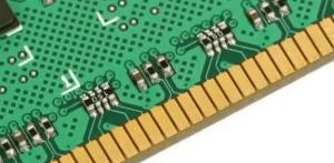
Memory modules such as DDR-series RAM use edge contacts to connect the module to a motherboard.
The gold-plated contacts provide a reliable interface while allowing the module to be inserted and removed when upgrading or servicing the system.
Expansion Cards
Computer expansion cards commonly use gold fingers to connect with motherboard slots.
Examples include:
- Graphics cards
- Network cards
- Sound cards
- Storage interface cards
- Industrial expansion cards
Communication Equipment
Communication systems may use edge-connector boards for modular system architectures.
Gold fingers can provide reliable connections between circuit boards and backplanes or connector assemblies.
Industrial Control Systems
Industrial control equipment often uses replaceable control cards and interface modules.
Gold fingers can support modular architectures in which individual boards can be removed for maintenance or upgrades.
Test and Development Equipment
Prototype platforms, development boards, and test fixtures may also use edge connectors where repeated insertion and removal is expected.
Why Gold Finger PCB Costs More Than Standard PCB Finishes
A Gold Finger PCB generally costs more than a conventional PCB with ENIG or other standard surface finishes.
Several factors contribute to the additional cost:
- Additional nickel and gold plating
- Higher plating requirements
- Special masking processes
- Edge preparation
- Beveling requirements
- Additional dimensional controls
- Specialized inspection
The cost difference is justified when the board requires repeated insertion, high contact reliability, and long-term resistance to corrosion and wear.
For applications that do not require repeated mechanical contact, standard surface finishes may be more economical.
Gold Finger PCB Design Checklist
Before manufacturing a gold finger board, engineers should confirm the following:
- Connector type and dimensions
- Gold finger length
- Contact width and spacing
- Gold and nickel plating requirements
- Edge bevel angle
- Board thickness
- Copper thickness
- Solder mask clearance
- Contact sequence
- Required insertion cycles
- Electrical requirements
- Mechanical tolerances
Clear specifications at the design stage can significantly reduce manufacturing problems and ensure compatibility with the mating connector.
Why Choose Kingda for Gold Finger PCB Manufacturing?
Kingda provides customized Gold Finger PCB manufacturing solutions for applications requiring reliable edge connections and repeated insertion and removal.
Gold finger production requires precise control of PCB fabrication, plating, edge dimensions, beveling, and electrical performance. Therefore, the manufacturing process should be evaluated together with the connector requirements from the beginning of the project.
Kingda can support customized PCB requirements involving:
- Gold finger PCB fabrication
- Hard gold plating
- Edge connector PCB structures
- Customized board dimensions
- Different gold finger lengths
- Segmented contact arrangements
- Multilayer PCB structures
- Controlled copper thickness
- Prototype and production requirements
- DFM engineering review
- Electrical testing and inspection
Engineering and Quality-Focused Manufacturing
Reliable gold finger performance depends on more than the appearance of the gold surface. Plating thickness, nickel barrier quality, contact geometry, bevel accuracy, PCB dimensional tolerances, and connector compatibility all influence the final result.
Kingda focuses on coordinating these requirements throughout the PCB manufacturing process to help customers achieve reliable electrical contact, mechanical durability, and consistent production quality.
Whether the application involves memory modules, expansion cards, industrial control boards, communication equipment, or other edge-connected electronic systems, selecting the correct PCB Gold Fingers structure and plating specification is essential for long-term performance.
Conclusion
A Gold Finger PCB is designed specifically for reliable electrical and mechanical connection through an edge connector. Its exposed contacts typically use a hard-gold plating system to provide good conductivity, corrosion resistance, and resistance to repeated mechanical wear.
Compared with standard PCB surface finishes, gold fingers require more specialized design and manufacturing processes, including plating control, edge preparation, beveling, and dimensional inspection.
For applications involving frequent insertion and removal, modular connections, or demanding connector reliability, properly designed Gold Finger PCB technology can provide a durable and stable interface.
Working with an experienced PCB manufacturer such as Kingda during the design and engineering stage can help ensure that plating specifications, connector dimensions, board construction, and manufacturing capabilities are properly matched to the final application.