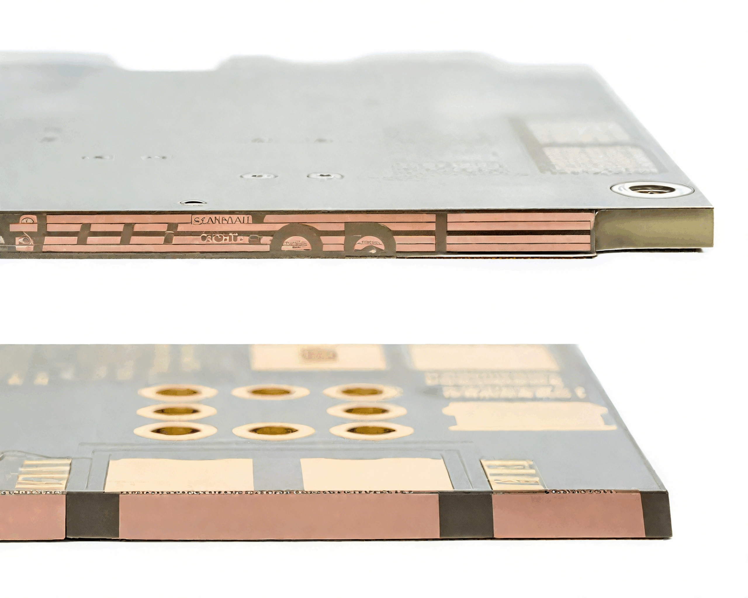
Ground Bounce: Design Rules and Process Limits
A single output switching produces a clean waveform, and the same device with an entire bus toggling at once produces intermittent receiver errors. The ground net is continuous, a multimeter reads a fraction of an ohm between the chip ground pin and the board ground, and yet the internal reference of the device is briefly no longer the same potential as the board it sits on. This is ground bounce, and it is a consequence of inductance rather than of a broken connection.
The mechanism is the same one that makes any voltage appear across an inductance when current changes: V equals L multiplied by the rate of change of current. When a driver pulls its output low, the load current has to return through the output transistor, the package ground pin, the solder ball, the via and the plane. Each of those elements carries parasitic inductance, and the transient current through them develops a voltage difference that shifts the chip internal ground reference relative to the board.
Why Simultaneous Switching Makes It Worse
The amplitude of the disturbance depends on how much current changes and how quickly. One output switching changes a modest current over an edge time in the region of a nanosecond. A parallel bus with sixteen or thirty-two outputs switching together changes a much larger current in the same time, so the product of inductance and current slope is multiplied. The reference shift grows with the number of simultaneously switching outputs, which is why the problem appears only when a bus is exercised.
The consequences are twofold. Outputs that reference the disturbed internal ground have their thresholds shifted, so a receiver may sample a one as a zero at the far end of the link. And any analogue function on the same die sees its reference move, which shows up as a glitch or a shift in a sampled value. Neither symptom appears in a static test, and neither is visible on a schematic, because the schematic models the ground as an ideal node.

Where the Loop Inductance Comes From
The return current does not travel through a single pin; it travels as a loop. The loop includes the output transistor, the package lead or ball, the board via, the plane beneath the device, the decoupling capacitor and its connection, and the path back into the supply. Every millimetre of that loop contributes inductance, and the parts that contribute most are the ones with the smallest cross section and the longest path, which in a ball grid array device are the vias and the ball-to-plane transition.
Reducing the loop means attacking several elements at once. More ground balls and more ground vias in parallel lower the effective inductance of the return path. Placing the decoupling capacitor so that its loop with the device supply pin is short keeps the high frequency current local instead of letting it travel to a remote capacitor. A solid reference plane directly beneath the device gives the returning current a wide, low inductance path, whereas a plane that is slotted or perforated by antipads forces the current to detour.
Design Measures That Reduce Bounce
The most effective measures reduce return inductance rather than change the driver. Increase the number of ground connections between the device and the plane, because inductance falls as conductors are placed in parallel, and place them as close as possible to the pins that switch the most current. Give each power and ground ball a via directly beside the pad rather than a short trace to a shared via, since a shared via couples the return currents of several pins together.
Decoupling and edge rate follow. Capacitors placed close to the supply pins with a short loop to ground keep the high frequency current local, and the plane beneath the device should be continuous in the region where the switching current returns. Where the reference plane must change, provide a nearby stitching via so the return current has a defined path instead of a long detour, following the same reasoning as the rules for ground current and harmonic distortion. Reducing the edge rate of a group of outputs in software, or adding a small series resistor, lowers the current slope and therefore the bounce directly; the trade is a slower transition that has to remain acceptable to the receiver.
Two further measures help at the system level. Staggering the switching of a wide bus so that not every output changes on the same clock edge spreads the current over time, which is a software decision rather than a hardware one. And keeping the device return path short relative to the board ground, as described in multilayer advantages for high speed design, ensures that the plane itself does not add inductance between the device and the point where the signal is referenced.
Verifying the Fix
Ground bounce is difficult to measure directly, because attaching a probe adds inductance to the very path being investigated. The practical method is to measure the consequence rather than the cause: monitor the device supply and ground pins with a probe whose own ground lead is as short as physically possible, and compare the waveform with the same measurement taken at a quiet point on the plane. The difference is the local reference shift. A near field scan of the device region shows where the disturbance is strongest, which helps when several devices share the board.
Verification should also reproduce the condition that created the problem. A pattern that toggles one output at a time will not show the effect, so the test must exercise a realistic bus pattern at the intended clock rate and check the receiver for errors rather than checking the driver output. Where the design has margin, an eye diagram measured at the receiver with all outputs switching simultaneously quantifies how much of the margin the bounce consumes.
Package and Die Level Contributions
Part of the problem is inside the device and cannot be fixed by layout. The bond wires or solder balls, the package substrate routing and the die level interconnect all add inductance between the silicon and the board, collectively described as package inductance. A device with a high pin count and many dedicated ground balls has a lower figure than a smaller package with few ground connections, which is why two parts with identical silicon can behave differently in the same socket. The escape routing that determines how much of that inductance is exposed to the board is covered in escape routing and fanout.
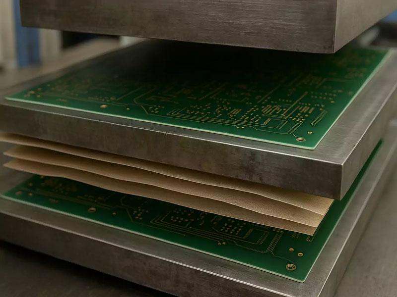
This is the reason a designer cannot always solve ground bounce by improving the board. If the package inductance dominates, adding vias and capacitors below the device produces diminishing returns, and the correct response is to reduce the current slope or select a package with more ground connections. Where the two contributions are comparable, the board measures still deliver most of the benefit, which is why quantifying the split with a measurement before choosing a fix saves time.
FAQ
Is ground bounce the same as a ground loop? No. A ground loop describes a potential difference caused by current flowing in a shared conductor between two points. Ground bounce is a transient reference shift caused by the inductance of the path between a device and the board, and it appears even when the ground network is properly connected.
Can a larger decoupling capacitor fix it? Usually not on its own. The inductance of the connection limits how fast the capacitor can supply current, so placement and loop area matter more than capacitance value. A large capacitor in the wrong position behaves like a remote reservoir.
Why does the problem only appear on some boards? Because the effect depends on the current slope and on the number of outputs switching, both of which vary with the software running on the device. A board that passes a functional test with a light bus pattern may fail with a heavy one.