HDI Design With 1 to 4 Order Blind and Buried Vias
Phones, tablets, wearables and high end industrial modules all rely on high density interconnect boards to fit the routing into the space available. Designing one is harder than designing an ordinary multilayer board, because the stack-up, the via strategy, the escape from the ball grid array and the impedance have to be planned together. The stack-up decides the signal quality and the manufacturing cost, and the via strategy decides the routing density and the yield, and both are settled at the beginning of the project rather than adjusted at the end.
What the Design Covers
Boards from a first order build up to a fourth order build-up are designed, including structures where any layer may be interconnected, across consumer, communications and industrial applications. The via plan is developed from the board thickness, the drill diameter and the layer count, so that the wiring density and the manufacturing cost are balanced against each other rather than one being maximised.
Fan-out is designed for ball grid arrays at a pitch of nought point four millimetres and above, including package on package and multichip modules, which is where the routing problem is usually concentrated. The impedance control is applied to the high speed signals, with single ended and differential values calculated against the actual stack-up so that what is designed can be produced.
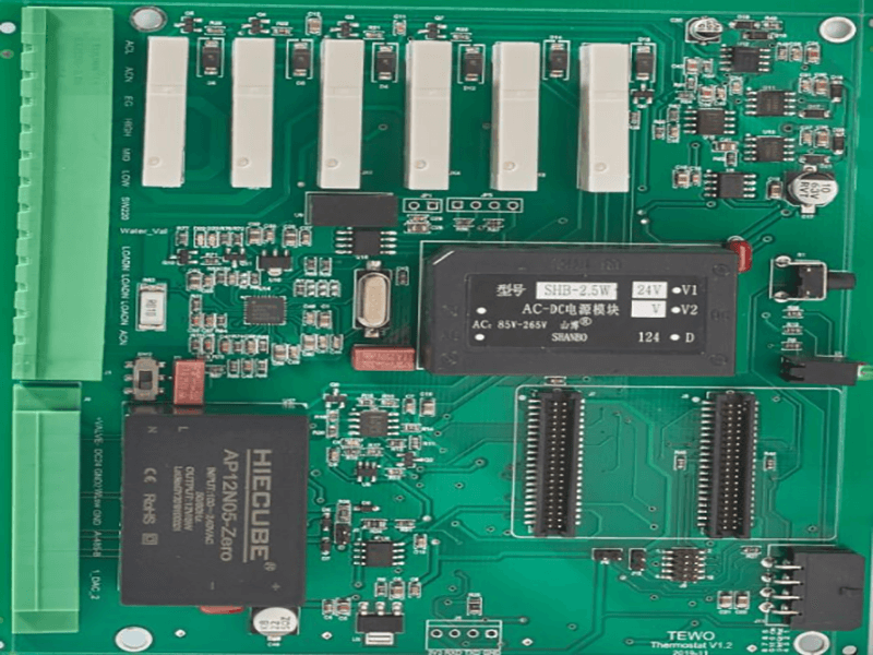
<img src="https://www.gopcba.com/wp-content/uploads/2026/05/Smart-Meter-PCBA.png" alt="HDI board design with blind and buried via structures” />
The Parameters
The design range covers first, second, third and fourth order HDI design, with any layer interconnection, and four to twenty layers. The finished thickness runs from nought point four to three millimetres. Laser drilled blind vias are drawn from nought point one to nought point one five millimetres, and the minimum trace width and spacing is three thousandths of an inch, subject to what the fabricator can achieve. Ball grid arrays are escaped from a pitch of nought point four millimetres, and the via filling is specified either as resin plugging under vacuum or as a plated fill.
Impedance tolerance is normally ten percent on standard material, and a tighter figure can be held on a material whose dielectric constant is more consistent.
Where the Design Decisions Are Made
The stack-up is the first decision, and it is the one that constrains everything else. The number of signal layers, the number of power and ground layers, the thickness, the impedance requirement and the via types are considered together, and more than one option is usually prepared so that the customer can choose between a cheaper construction and one that gives more routing freedom.
The via strategy follows. Blind vias, buried vias and through vias are combined according to where the components are and where the signals have to travel, and the combination determines both the density that can be reached and the number of process steps. The choice between a resin filled via and a plated fill, and whether a via in pad is required, belongs to the same decision, and the process feasibility is confirmed with the fabricator while the design can still change.
Escaping a dense array is the third decision. At nought point four millimetres the usual answer combines a laser blind via with a via in pad structure, and the design of the pad, the via, the routing channel and the soldermask definition all have to be settled together so that the routing passes and the joint remains reliable.
The power and ground planes are the fourth. A board with many layers and a high component density needs its planes divided deliberately, because a division that follows the components rather than the current paths raises the impedance of the supply network and lengthens the return path, which affects both the signal integrity and the compatibility behaviour.

Design and Fabrication Working Together
Because the same group also manufactures high density interconnect boards, the review at the design stage is carried out with the process in view. The manufacturability of the panel, the stencil and the stack-up is checked while the layout is being developed, the stack-up and the impedance are confirmed by the designer and the fabrication engineer together, and the design parameters are kept aligned with the process parameters so that the calculation matches what the factory will build.
When a question arises during production, it goes to the designer who drew the board rather than to a third party, and the boards move from fabrication to SMT assembly without being packed and reopened. A first order board is produced with registration between layers held within about twenty five micrometres, and the whole flow is recorded under quality management.
Two Typical Projects
A six layer second order board for a phone main board carried a controller in a nought point four millimetre ball grid array on a one millimetre board. The fan-out used blind vias and vias in pad, the impedance was controlled for signals running at several gigabits per second, and the board went from design into fabrication and assembly in the same group and passed on the first prototype.
An eight layer third order board for an industrial controller carried several high speed links and a power management section on a one point six millimetre board. The difficulty was the combination of a high routing density with operation across a wide temperature range, and the answer was a stack-up with a deliberate plane arrangement and a supply network whose impedance was verified before the artwork was released.
What to Send
The schematic, the component data with the package drawings for the dense devices, the mechanical requirements including the thickness, the outline and the forbidden areas, the impedance requirement and any preference in the stack-up are the starting point. Where a preliminary stack-up already exists it can be supplied, and the assessment builds on it. The more complete the data, the more reliable the estimate and the schedule. Our PCB design and layout group carries out the work and PCB manufacturing produces the board.
Why the Two Decisions Cannot Be Separated
`r`n
A stack-up chosen for cost and a via plan chosen for density are not independent. Each build-up step adds a lamination and a laser drilling operation, so a plan that uses a higher order than the routing needs pays for process steps it does not use, while a plan that uses a lower order than the density requires leaves signals that cannot be escaped at all. The two are therefore evaluated together at the start, against the actual device data rather than against a rule of thumb for the layer count.
`r`n
The same applies to the impedance. A width that produces the correct impedance on one stack-up produces the wrong value on another, so the width table is generated after the stack-up is fixed and not before. A project that calculates the widths first and then changes the construction has to go back and recalculate every controlled net.
FAQ
How much more does a high density design cost? A first order design is roughly thirty to fifty percent above an ordinary board of the same layer count, and higher orders cost more, because the via planning, the fan-out and the stack-up work are all greater.
How long does it take? A six to eight layer board of moderate complexity takes one to two weeks, and a board of ten or more layers with many high speed signals takes two to four weeks, with simulation adding further time.
Can the board be produced by the same group? Yes, from the first order to the fourth, with the layers registered within about twenty five micrometres.