HDI Fabrication: Stacked and Staggered Blind Vias
As products become thinner and smaller, an ordinary through hole board runs out of routing space. The answer that HDI fabrication provides is to drill vias that do not pass through the whole construction: a blind via reaches from an outer layer to an inner one, a buried via connects inner layers only, and both are produced by laser drilling and successive lamination. The result is more routing in the same area, a smaller board and, in many cases, a better signal path.
What the Process Covers
Constructions from a first order build-up to a fourth order build-up are produced, including both stacked and staggered blind vias, with a total layer count from four to thirty. Laser drilled blind vias are made down to nought point one millimetres, or four thousandths of an inch, using a carbon dioxide laser process, and mechanically drilled buried vias down to nought point two millimetres. The minimum trace width and spacing on an inner layer is three thousandths of an inch.
Layer registration is held within about twenty five micrometres across all the lamination cycles, which is the figure that decides whether a blind via lands on its pad. The dielectric between layers can be as thin as nought point zero eight millimetres on a thin construction. The surface finish is selected from immersion gold, OSP, immersion silver and immersion tin, the material from FR4, high glass transition FR4 or halogen free laminate, and the finished thickness runs from nought point four to three point two millimetres.
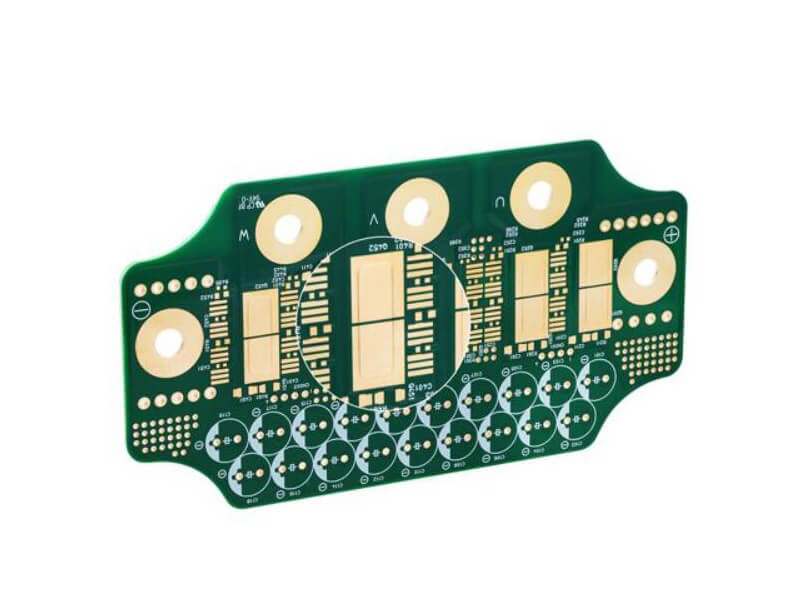
<img src="https://www.gopcba.com/wp-content/uploads/2024/09/BO7B6934.jpg" alt="HDI board with blind and buried via structures” />
The Build-Up Sequence
The inner layer cores are produced first. The layers that will contain buried vias are laminated together, and those vias are drilled and plated. The outer patterns follow, and then the build-up begins: a laser drills the blind vias from the outer layer to the layer beneath, the vias are metallised and plated, and the next layer is added.
Each order of blind via corresponds to one lamination and one laser drilling cycle, which is the reason the cost rises with the order. A higher order means more cycles, a tighter requirement on the registration between them, and a lower yield, because a deviation that would be absorbed on a simple board accumulates across the successive laminations. The process control that makes the difference is a stable lamination and alignment system, laser parameters matched to the material and the thickness, and an inspection point after each critical step.
Where the Boards Are Used
Smartphones use them for the main board and for module boards, where the controller is a large ball grid array and the space is fixed. Wearables such as watches and bands need the routing density in a board that is both small and thin. Camera modules and tablets use them for the same reasons. Communications equipment uses them in base stations and modules where the channel count is high, and medical devices use them where the instrument has to be small without giving up the performance.
How the Quality Is Held
Registration is the first control. Each lamination is measured for its offset, and the measurement is used to keep the accumulated deviation inside the twenty five micrometre figure, because a blind via that misses its pad produces either an open circuit or a short that appears later rather than during the electrical test.
Laser parameters are the second. Different materials and different dielectric thicknesses need different settings, and the machine is calibrated for each combination so that the hole is correctly shaped and its wall is clean, which is what allows the subsequent copper plating to adhere. A hole with a rough or contaminated wall may pass the electrical test and fail in the field.
Detection runs through the process rather than at the end. Optical inspection is applied after the inner layer, after the outer layer, and again later in the flow, and a flying probe test confirms the electrical connectivity of the finished board. Acceptance follows the IPC-A-600 standard for printed board acceptability.
Reliability testing is available where the product requires it: impedance measurement, thermal stress, microsection analysis and other reliability checks that verify the structure rather than only its appearance. A microsection is the only method that shows what the barrel of a blind via actually looks like, and on a high order construction it is worth doing.
What the Design Should Consider
The stack-up belongs to the discussion with the fabricator, because the dielectric thickness that a build-up can produce decides the impedance that can be achieved. Whether the vias are stacked or staggered follows from the pitch of the ball grid array and the routing that has to escape, and the trace width and the pad dimensions have to be inside the process capability rather than at its edge.
Because the same group also designs high density boards, the review can happen while the layout is still being drawn. A stack-up that cannot be produced, or a via structure that exceeds the registration tolerance, is found before the artwork is released. Our PCB manufacturing group runs the build-up process, PCB design and layout covers the design, and the boards continue into SMT assembly without being packed and reopened, with the records held under quality management.
What the Customer Should Send
`r`n
The Gerber data are the starting point, together with the number of build-up orders required and the layer count. The stack-up, if one has been defined, allows the dielectric thicknesses and the impedance targets to be checked against what the process can produce, and where the stack-up is still open, the number of signal layers, the power and ground layers and the board thickness are enough to propose one.
`r`n
Stating the via sizes that the design assumes matters, because a via drawn at the process limit leaves no room for the normal variation of the line. Where a ball grid array has to be escaped, the pitch and the pin count decide whether the blind vias are stacked or staggered, and that decision changes both the routing and the number of lamination cycles.
`r`n
For a high order construction it also helps to say which features are essential and which are preferences. A design that needs a fourth order build-up across the whole board and one that needs it only under the controller are very different orders, and the second is considerably cheaper to produce.
`r`n
Where the Yield Comes From
`r`n
The yield on a high density board is not a single number that the factory has or does not have. It is the product of the registration at every lamination, the condition of the laser drilling, the quality of the plating in the small barrels and the discipline of the inspection between the steps. A deviation that would be tolerable on an ordinary multilayer board is not tolerable here, because it accumulates, and a defect that appears after several lamination cycles has already consumed the value of everything before it.
`r`n
That is the reason the inspection points are placed after each critical operation rather than only at the end. A board that is found to be outside tolerance after the second lamination is scrap, and a board that is found to be outside tolerance after the fifth has cost considerably more to produce.
FAQ
What does the order of a high density board mean? It is the number of build-up layers of blind vias. A first order board has one such layer, a second order board adds another that may be stacked on the first or offset from it, and an any layer construction stacks several, which is what gives the highest density.
How much more does it cost? The cost rises with the order, because each order adds a lamination, a laser drilling step and a plating step, and the yield falls as the structure becomes more complex.
How small can a laser via be? Nought point one millimetres, with nought point one and nought point one five millimetres being the common sizes. The limit depends on the thickness of the board and the dielectric.