



High Current PCB Design: Width, Copper and Heat
Sooner or later a design has to move more current than a comfortable trace width allows. A motor driver, a battery charger, a distribution rail or a heater all push the copper toward the point where one millimetre per ampere stops being practical and the layout has to change shape. The copper becomes the component: its width, its thickness and its temperature rise decide whether the board works, whether it survives, and whether the enclosure around it stays within its own limits. This guide covers the factors that set the copper geometry and the layout techniques that keep heat out of the parts that cannot take it.
What Sets the Copper Geometry
Every high current PCB design starts from three parameters that decide how much current a trace can carry: its cross sectional area, the temperature rise that is acceptable, and the environment the board sits in. Cross sectional area is width multiplied by thickness, so either can be increased, and the choice between them is a manufacturing question as much as an electrical one. The environment matters because a trace in still air at sixty degrees ambient has far less headroom than the same trace in a ventilated enclosure at room temperature.
A common rule of thumb allows about one millimetre of width per ampere for standard one ounce copper with a modest temperature rise. That figure is only a starting point. A ten ampere rail built to that rule needs ten millimetres of copper, which is often impossible, and the answer is then to use heavier copper, more layers, or a different structure entirely such as a bus bar or a metal core.
Copper Thickness and Cost
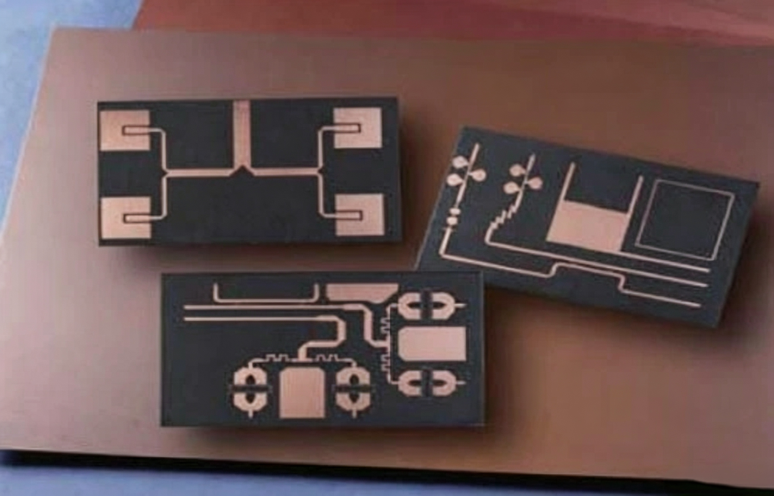
Standard copper on an inner layer is half an ounce after lamination, and outer layers commonly start at one ounce, which is about thirty five micrometres. Two, three and four ounce copper are all available, and each step reduces the width needed for the same current. The penalty is that heavier copper is harder to etch, so minimum feature sizes widen, and cost rises with plating time and process difficulty rather than with the metal itself.
The fabricator capability matters twice over. Outer layer copper thickness is set by the plating process and is usually quoted as a minimum on the finished trace, while inner layer thickness is fixed by the foil the shop stocks. A design that assumes a heavy inner layer without confirming the stock will be built thinner than intended, and the current capacity quietly disappears. Our notes on trace width and current calculation cover the arithmetic.
Power Dissipation and Temperature Rise
Losses in a trace follow the relationship between resistance and current: power equals current squared multiplied by resistance. Because the current term is squared, doubling the current quadruples the heat, which is why high current designs move so quickly from comfortable to critical. Resistance itself rises with temperature, so a trace that heats up becomes more resistive and dissipates more, and the system can run away if the copper is marginal.
Heat has consequences beyond the trace. Local hot spots cause the laminate to expand unevenly, which distorts the board, stresses plated barrels and can eventually crack a layer or a joint. A hot spot under a connector or a shunt also drifts the measurement that the circuit depends on, so thermal and electrical design have to be considered together rather than in sequence.
Layout Rules for Power Paths
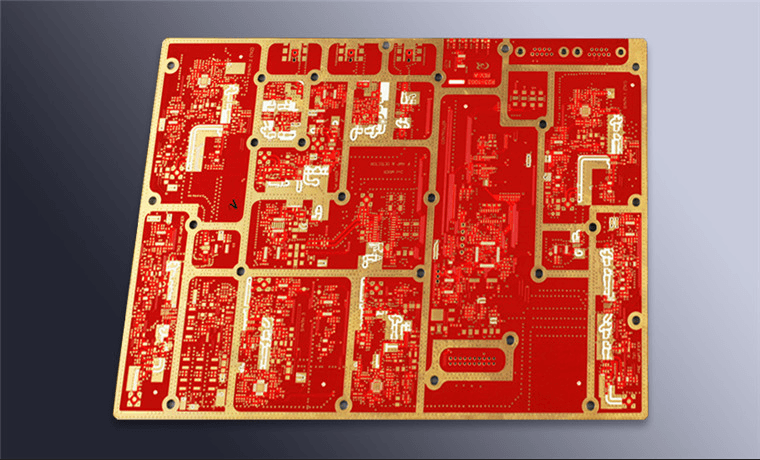
Keep the high current path short. Every millimetre of length adds resistance and therefore loss, and the loss is proportional to the square of the current. Where a long run is unavoidable, widen the conductor along its whole length rather than only near the terminals, because a narrow section anywhere in the path becomes the limiting element and the hot spot.
Use copper pours liberally. A polygon at a defined net carrying the supply has far more area than a trace and spreads heat as well as current, and it is easy to widen later. Where a device has many power pins in a fine pitch package, place the pour directly beneath the package and connect it with a via array, which keeps the current path short and the inductance low. Our notes on power plane design describe how the planes fit into this.
Thermal Isolation of Sensitive Parts
Analogue to digital converters, voltage references and precision amplifiers all drift with temperature. On a board that carries substantial current, those parts have to be physically separated from the heat sources, and the copper around them has to be arranged so that heat does not simply conduct across the plane to reach them.
The techniques are straightforward: keep the sensitive parts away from the power stage, avoid filling copper beneath them so that the plane does not become a heat spreader, use thermal relief connections where a pad must still be connected, and where the layout allows, cut slots in the board to break the conduction path. Each of these changes the mechanical or electrical design slightly, so they should be decided early rather than added after a thermal survey.
Reinforcing a Trace with Solder
Opening the solder mask over a trace and adding solder is an old and effective way to increase current capacity at almost no cost. The solder adds cross sectional area and lowers resistance, and because it is applied during assembly the process needs no extra fabrication step. It is widely used on motor drivers, power supplies and any board where a few amperes have to cross an area too small for heavy copper.
The technique has limits. Solder resistance is higher than copper, so the gain is smaller than the added thickness suggests, and the profile becomes uneven, which can affect impedance and appearance. It also only works where the trace will be reflowed or wave soldered, so it is not available on a fully assembled board being reworked by hand.
Vias, Connectors and Terminations
The conductors that connect to the trace are often the real bottleneck. A single small via has a fraction of the cross section of a wide trace, and a connector rated for its current in free air may be rated for much less when it is surrounded by other contacts. Vias in a power path should be used in arrays, with the count calculated from the current and the individual via rating rather than assumed.
Terminations deserve a second look as well. Solder joints add resistance, connector contacts add more, and the temperature rise at a contact is usually worse than in the trace leading to it. Where a rail carries tens of amperes, the connection is often the item that decides the rating of the whole path.
Verifying the Design
Calculation gets the design close, and measurement confirms it. A thermal image of the board under full load shows where the heat actually concentrates, which is rarely exactly where the calculation predicts, and a voltage drop measurement across the power path gives the real resistance including joints and connectors. Both are cheap compared with a field failure.
Where the design will run at high current continuously, a load test at elevated ambient temperature is worth more than any room temperature check. Copper that is comfortable at twenty five degrees may be marginal at sixty, and a design verified only in the laboratory can still fail in a cabinet. Our notes on PCB thermal design rules set out the wider thermal picture, and copper plating and via filling describes what the fabricator can guarantee.
FAQ
How wide should a high current trace be? Width follows from the current, the copper thickness and the acceptable temperature rise. A rough starting point is one millimetre per ampere for one ounce copper, but the figure must be checked against the real copper weight and the actual ambient.
Is heavier copper worth the extra cost? It usually is when board area is limited, because four ounce copper carries roughly four times the current of one ounce at the same width. The cost is driven by etching difficulty rather than by the metal, so the trade should be priced before the stackup is fixed.
Can solder really increase a trace rating? Yes, adding solder over exposed copper lowers resistance and increases capacity, and it is common practice on power boards. The gain is modest because solder is more resistive than copper, and the surface becomes uneven.


