HDI Microvias: Types, Benefits, Design Challenges & PCB Manufacturing
As modern electronic devices such as smartphones, laptops, tablets, and wearable electronics continue to become smaller while delivering higher performance, advances in PCB technology have become increasingly important. Many of these high-performance products rely on HDI PCB technology to integrate a large number of components and electrical connections within a limited area.
When board space is restricted, every millimeter of the PCB layout matters. One of the key technologies used to maximize routing density in HDI multilayer boards is the microvia.
As the name suggests, a microvia is an extremely small-diameter via typically formed using laser drilling. Microvias are generally much smaller than conventional through-hole vias and are commonly used to establish short electrical connections between adjacent PCB layers. Their compact dimensions allow designers to achieve higher interconnection density while reducing the amount of board space consumed by vias.
For engineers working on high-density PCB Design, understanding microvia structures, their advantages, manufacturing requirements, and potential challenges is essential for developing reliable and manufacturable HDI boards.
What Is a Microvia in an HDI PCB?
A microvia is a small-diameter interconnection used primarily in HDI PCB structures. Unlike conventional mechanical through-holes, microvias are typically produced using laser drilling and are designed to connect an outer layer to an adjacent inner layer or between selected layers within a sequentially laminated structure.
Because microvias occupy less space than conventional vias, they allow PCB designers to place traces and component pads more efficiently. This is particularly valuable when routing high-density circuits in compact electronic products.
Microvias can also reduce the electrical path length between layers. When properly designed and manufactured, this can contribute to improved signal integrity, lower parasitic effects, and better performance in high-speed and high-frequency applications.
Types of Microvias Used in HDI PCBs
Different microvia structures can be used depending on the HDI stackup, routing requirements, electrical performance, and manufacturing capabilities. The most common structures include buried microvias, blind microvias, stacked microvias, and staggered microvias.
Buried Microvias
Buried microvias are used to connect internal layers of an HDI PCB without extending to the external surface of the board. As their name suggests, they are embedded within the internal layer structure and cannot normally be seen from the outside.
By connecting selected internal layers, buried microvias provide additional routing paths without occupying valuable surface area. This allows engineers to route more signals through a compact multilayer structure and create additional space for components and surface traces.
Buried microvias can also contribute to electrical performance in several ways. Their short interconnection paths can reduce parasitic inductance and minimize unnecessary signal discontinuities. Keeping certain signal connections within internal layers can also help with electromagnetic compatibility when combined with an appropriate stackup and reference-plane design.
Blind Microvias
Blind microvias connect an external PCB layer to one or more internal layers without passing completely through the circuit board. They can therefore provide a direct connection from the component side or solder side to selected layers within the HDI stackup.
Blind microvias are particularly useful for fan-out routing around fine-pitch components. They allow designers to escape signals from dense component areas without consuming the full vertical space of a conventional through-hole via.
Compared with buried structures, blind microvias are exposed to the outer surface and may experience different mechanical and thermal stresses during PCB assembly and operation. Their depth, diameter, aspect ratio, plating quality, and position within the stackup therefore require careful consideration during PCB Design and PCB Manufacturing.
Stacked Microvias
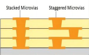
Stacked microvias are formed by placing multiple microvias vertically on top of one another. The microvias are typically interconnected through copper-filled structures, allowing electrical connections between non-adjacent layers.
Stacked microvias provide excellent vertical interconnection density and are particularly useful in complex HDI stackups. They can significantly reduce the horizontal routing area required for layer-to-layer connections, making them suitable for highly compact PCB designs.
However, stacked structures require tighter manufacturing control than simpler microvia configurations. Copper filling, alignment, lamination, drilling accuracy, and interlayer registration must all be carefully controlled to achieve reliable connections.
Staggered Microvias
Staggered microvias are arranged so that successive microvias are offset rather than vertically aligned. In other words, the microvias are positioned in a staggered pattern across different layers.
This configuration can reduce some of the manufacturing and mechanical challenges associated with directly stacking multiple microvias. Staggered structures can provide good mechanical reliability while still offering substantially higher routing density than conventional through-hole interconnections.
The appropriate configuration depends on the required electrical performance, available board space, stackup structure, and manufacturing capabilities.
Benefits of Microvias in HDI PCBs
Microvia technology provides several important advantages in terms of miniaturization, electrical performance, signal integrity, and routing flexibility.
Smaller Size and Lower Weight
One of the primary advantages of microvias is their compact footprint.
Because microvias occupy significantly less PCB real estate than conventional vias, engineers can route more signals through the same board area. This makes it possible to reduce PCB dimensions while maintaining or increasing circuit functionality.
This advantage is particularly important in smartphones, tablets, wearable devices, portable medical equipment, and other compact electronic products where PCB size and weight are critical design constraints.
Higher Routing Density
Microvias enable much denser interconnections than traditional via structures. Their small diameter allows them to be positioned closer to fine-pitch component pads and traces.
This makes microvias especially useful for high-density component packages such as BGAs and other fine-pitch devices. By improving fan-out capability, microvias can reduce routing congestion and make better use of available PCB layers.
Improved Electrical Performance
The shorter interconnection path associated with microvias can reduce parasitic electrical effects compared with larger conventional via structures.
Depending on the application and overall stackup design, microvias can help reduce parasitic inductance and capacitance while minimizing unnecessary discontinuities in high-speed signal paths.
For high-speed PCB Design, these characteristics can contribute to more predictable electrical behavior.
Better Signal Integrity
Signal integrity becomes increasingly important as operating frequencies and data rates increase.
Microvias can shorten vertical transitions between PCB layers, reducing the length of the electrical path. Their smaller physical dimensions can also reduce unwanted parasitic effects.
When combined with controlled impedance routing, appropriate reference planes, optimized layer transitions, and proper grounding techniques, microvias can support reliable high-speed signal transmission.
However, microvias alone do not guarantee good signal integrity. The complete PCB stackup, trace geometry, dielectric properties, return-current path, via arrangement, and component placement must all be considered.
Improved Mechanical Reliability
Microvia structures can also contribute to the mechanical reliability of an HDI board when properly designed and manufactured.
A well-designed distribution of interconnections can help optimize the use of available board space and reduce unnecessary mechanical concentration around individual areas. Manufacturing quality is equally important because defects in copper plating, filling, lamination, or layer registration can negatively affect long-term reliability.
For demanding applications, engineers should evaluate thermal cycling, mechanical stress, via fatigue, and interlayer adhesion as part of the overall reliability strategy.
More Efficient Use of PCB Materials
Although microvia fabrication requires specialized processes such as laser drilling and, in some structures, copper filling, microvias can enable a more compact overall board architecture.
A smaller PCB may require less laminate, copper, and other materials. In certain designs, microvias can also reduce the need for additional board layers by providing more efficient vertical interconnections.
Therefore, the total cost impact should be evaluated at the complete product level rather than by comparing the cost of microvia fabrication alone.
Challenges in Microvia PCB Design
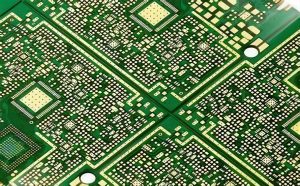
Despite their advantages, microvias introduce additional PCB Manufacturing and reliability considerations. Engineers should address these issues during the initial design stage rather than attempting to correct them after fabrication.
Aspect Ratio Control
The aspect ratio of a microvia generally refers to the ratio between its depth and drilled diameter.
An excessively high aspect ratio can make reliable copper plating and filling more difficult. It may increase the risk of incomplete plating, voids, cracking, or other reliability problems.
For this reason, microvia dimensions should be selected according to the capabilities of the PCB manufacturer and the requirements of the applicable design and manufacturing standards.
A commonly used design target for microvias is approximately a 1:1 depth-to-diameter ratio, although the actual acceptable value depends on the fabrication process, material system, copper plating technology, and manufacturer capabilities.
Thermal Management
HDI PCBs often contain a high concentration of components and interconnections within a relatively small area. As component density and power consumption increase, thermal management becomes an important design consideration.
Microvia structures themselves can also influence thermal behavior. Thermal microvias may be used to transfer heat away from high-power components toward internal copper planes or other thermal-management structures.
Engineers should consider copper distribution, thermal vias, copper planes, dielectric materials, component placement, and external heat dissipation mechanisms when developing the complete thermal design.
Material Selection
Material selection is critical for reliable microvia fabrication.
HDI boards commonly use materials and dielectric systems designed to support sequential lamination, laser drilling, fine-line routing, and controlled electrical performance. The material must be compatible with the selected laser-drilling process and the required thermal and mechanical conditions.
For high-speed applications, dielectric constant, dissipation factor, thermal stability, coefficient of thermal expansion, moisture resistance, and dimensional stability should also be evaluated.
Rather than selecting a material solely based on thermal conductivity, engineers should consider the complete electrical, thermal, mechanical, and manufacturing requirements of the application.
Choosing the Appropriate Microvia Structure
The appropriate microvia structure depends on the PCB’s electrical requirements, available space, stackup, reliability targets, and manufacturing capabilities.
Stacked microvias can provide very high vertical interconnection density and are useful when routing space is extremely limited. However, they generally require more complex manufacturing processes and tighter process control.
Staggered microvias can provide an alternative approach with different mechanical and manufacturing characteristics.
Blind and buried structures may also be combined with stacked or staggered configurations to create sophisticated HDI architectures.
Therefore, the microvia structure should be selected during the early stages of PCB Design, with input from the PCB manufacturer whenever possible.
HDI Stackup Design
The HDI stackup is one of the most important factors affecting microvia performance.
Engineers must coordinate microvia locations with the overall multilayer stackup, including:
- Dielectric thickness
- Copper thickness
- Microvia diameter and depth
- Layer-to-layer registration
- Signal and reference-plane arrangement
- Microvia stacking or staggering configuration
- Sequential lamination requirements
- Controlled impedance requirements
- Thermal management structures
A poorly optimized stackup can create routing difficulties, impedance discontinuities, manufacturing problems, or reliability risks.
For this reason, stackup planning should be performed together with PCB Design and PCB Manufacturing engineering teams.
Microvias vs. Traditional Through-Hole Vias
The primary difference between microvias and conventional through-hole vias is their physical structure and manufacturing method.
Traditional through-hole vias typically extend through the entire PCB, regardless of how many layers need to be connected. This can consume valuable routing space on every layer through which the via passes.
Microvias, by contrast, connect only selected layers. Their smaller diameter and limited depth provide greater flexibility for high-density routing.
| Feature | Microvias | Traditional Through-Hole Vias |
|---|---|---|
| Typical drilling method | Laser drilling | Mechanical drilling |
| Connection depth | Selected layers | Usually entire board |
| Footprint | Very small | Larger |
| Routing density | High | Lower |
| Fine-pitch component routing | Highly suitable | More restrictive |
| HDI applications | Common | Limited for very dense designs |
| Manufacturing complexity | Higher | Generally lower |
| Cost per structure | Higher | Generally lower |
The choice between the two depends on the board architecture. Microvias are not necessarily a replacement for every conventional via; instead, both technologies can be combined to create an optimized PCB interconnection structure.
Microvia Manufacturing Process
Reliable microvia performance depends heavily on manufacturing quality. A typical HDI microvia manufacturing process may include several key stages:
- Material preparation – Appropriate dielectric and copper materials are selected according to the required HDI stackup.
- Sequential lamination – Additional dielectric and copper layers are laminated to build the required multilayer structure.
- Laser drilling – Microvias are formed using a controlled laser-drilling process.
- Desmear and cleaning – Residues generated during drilling are removed to prepare the hole surface.
- Copper plating – The microvia walls are metallized to establish electrical conductivity.
- Copper filling – For stacked microvia structures, conductive copper filling may be required to create reliable interconnections.
- Additional lamination and processing – Further HDI build-up layers may be added depending on the stackup.
- Inspection and testing – AOI, electrical testing, cross-section analysis, and other inspection methods can be used to verify manufacturing quality.
Because microvias are extremely small, process control is critical. Laser energy, drilling accuracy, copper plating thickness, filling quality, registration, and lamination parameters must be tightly controlled.
How to Improve Microvia Reliability
Several design and manufacturing practices can improve the reliability of HDI microvias:
- Follow the PCB manufacturer’s minimum microvia dimensions and spacing.
- Maintain an appropriate microvia aspect ratio.
- Avoid unnecessarily aggressive stacked-via structures.
- Optimize copper filling for stacked microvias.
- Maintain accurate layer-to-layer registration.
- Select materials compatible with sequential lamination and laser drilling.
- Consider thermal expansion during material selection.
- Use appropriate copper thickness and plating specifications.
- Perform cross-section analysis during qualification.
- Apply reliability testing appropriate to the final application.
Early collaboration between the PCB designer and manufacturer can significantly reduce manufacturing risks.
Applications of HDI Microvias
Microvia technology is widely used in products where high functionality must be achieved within a compact form factor.
Typical applications include:
- Smartphones and tablets
- Laptops and compact computing systems
- Wearable electronics
- Medical electronic devices
- Automotive electronics
- Telecommunications equipment
- High-speed networking hardware
- Consumer electronics
- Industrial control systems
- Portable electronic equipment
As electronic products continue to become smaller and more powerful, the demand for high-density interconnection technologies is expected to remain important in advanced PCB Manufacturing.
Conclusion
Microvias are a fundamental technology for modern HDI PCB design. By providing compact layer-to-layer interconnections, they enable engineers to achieve higher routing density, smaller board dimensions, improved high-speed electrical performance, and more efficient use of PCB space.
However, the benefits of microvias depend heavily on proper design and manufacturing control. Aspect ratio, material selection, stackup architecture, copper plating, filling, thermal management, and layer registration must all be carefully considered.
For engineers developing compact, high-speed, and high-density electronic products, selecting the appropriate microvia structure and working with an experienced PCB Manufacturing partner can help balance miniaturization, electrical performance, reliability, and production requirements.
Article Summary
HDI microvias provide a compact and efficient method for connecting selected layers in high-density multilayer PCBs. Buried, blind, stacked, and staggered microvias each offer different structural and manufacturing characteristics. Their small size enables higher routing density and supports the miniaturization of modern electronic devices. At the same time, successful microvia implementation requires careful control of aspect ratio, material selection, thermal performance, stackup design, copper plating, and manufacturing tolerances. By integrating microvia considerations into the early stages of PCB Design and PCB Manufacturing, engineers can develop compact and reliable HDI circuit boards for demanding electronic applications.