



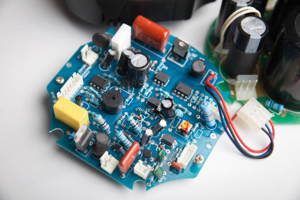
High Frequency Rogers PCB Manufacturing Process | Advanced RF PCB Solutions
In high-frequency communication applications, Rogers materials have become a preferred choice for advanced printed circuit boards due to their low dielectric constant, low dissipation factor, and excellent thermal stability. These properties make High Frequency Rogers PCB solutions ideal for demanding applications such as 5G communication systems, satellite equipment, radar systems, and high-speed RF electronics.
Compared with traditional FR4 circuit boards, Rogers PCB manufacturing requires more precise process control because high-frequency signals are extremely sensitive to material properties, impedance variations, surface roughness, and dimensional changes. Proper fabrication methods are essential to maximize electrical performance and ensure reliable signal transmission.
As a professional PCB and PCBA manufacturer, gopcba provides integrated solutions covering PCB fabrication, assembly, testing, and production support. From prototype development to volume manufacturing, advanced process management ensures consistent quality for high-performance electronic applications.
For customers requiring complete electronic manufacturing solutions, gopcba also provides PCB Manufacturing Services including multilayer PCB fabrication, high-frequency PCB production, and customized circuit board manufacturing.
The manufacturing process of Rogers-based high-frequency PCBs must consider both material characteristics and high-frequency electrical requirements. The complete process mainly includes six critical stages.
The first step in Rogers PCB Manufacturing is selecting the appropriate Rogers laminate according to electrical performance requirements, including dielectric constant (Dk), dielectric loss, thickness, thermal characteristics, and application frequency.
Common Rogers materials include:
- Rogers RO4350B
- Rogers RO4003C
- Rogers RT/duroid series materials
Each material has different electrical characteristics and must be matched with the PCB design requirements.
Before production begins, incoming materials undergo strict inspection. Manufacturers check surface quality, thickness consistency, and possible defects caused by transportation or storage, such as scratches, contamination, or oxidation.
Unlike conventional FR4 materials, Rogers laminates often have smoother surfaces and different mechanical properties. Therefore, special handling procedures are required during storage and processing to prevent surface damage.
The inner layer circuit is the foundation of signal transmission in multilayer Rogers PCBs. High precision manufacturing technology is required to maintain circuit accuracy and signal integrity.
The main steps include: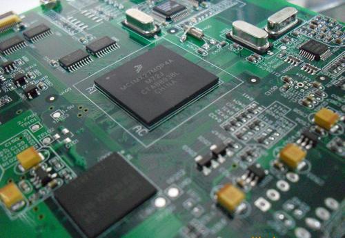
High-performance dry film is applied to the copper surface using vacuum lamination equipment. This process ensures complete adhesion between the film and substrate while preventing air bubbles or uneven coverage.
Laser Direct Imaging (LDI) technology is commonly used to transfer circuit patterns accurately onto the dry film. Compared with traditional exposure methods, LDI provides better alignment accuracy and supports fine-line circuit manufacturing.
This is especially important for RF circuits where small variations in trace width can affect impedance performance.
After exposure and development, unwanted copper is removed through controlled chemical etching.
The etching process requires precise control of:
- Chemical concentration
- Etching temperature
- Spray pressure
- Etching speed
After etching, Automated Optical Inspection (AOI) equipment is used to detect possible defects, including:
- Open circuits
- Short circuits
- Missing traces
- Line width deviations
This ensures the reliability and accuracy of inner-layer circuits.
Lamination is one of the most critical stages in Rogers PCB fabrication because it directly affects mechanical reliability, impedance performance, and long-term stability.
When combining Rogers materials with FR4 layers, manufacturers must carefully control material compatibility because different materials have different:
- Thermal expansion coefficients
- Resin systems
- Mechanical properties
The multilayer stack-up design must be calculated according to impedance requirements. Proper prepreg selection between Rogers laminates and FR4 layers helps improve bonding strength while maintaining electrical performance.
For complex electronic products requiring both PCB fabrication and assembly, gopcba offers professional PCB Design & Layout Services to optimize layer structures, signal routing, and high-frequency performance before manufacturing.
Engineers analyze:
- Signal layer arrangement
- Dielectric thickness
- Copper thickness
- Controlled impedance requirements
A precise stack-up design reduces signal loss and improves high-frequency transmission performance.
Rogers PCB lamination requires carefully controlled temperature and pressure profiles.
A step-by-step heating and pressing process is used to prevent:
- Material deformation
- Layer separation
- Internal stress accumulation
Proper lamination parameters ensure stable electrical characteristics throughout the PCB lifespan.
High-frequency signals are highly sensitive to via performance. Poor drilling quality can increase signal loss and reduce PCB reliability.
Because Rogers materials have different hardness and mechanical characteristics compared with FR4, drilling parameters must be optimized.
Manufacturers carefully adjust:
- Drill speed
- Feed rate
- Tool selection
- Drilling depth
Using appropriate carbide drill bits helps minimize:
- Burr formation
- Resin contamination
- Hole wall damage
After drilling, chemical copper deposition creates a conductive layer inside the holes. Electrolytic copper plating is then applied to increase copper thickness and improve electrical conductivity.
A stable hole metallization process ensures reliable signal transmission and mechanical strength.
For applications requiring complete prototype-to-production support, gopcba provides Rapid PCBA Prototyping Services to accelerate product development and verification.
The outer layer circuit directly affects signal transmission quality and electrical stability. For High Frequency Rogers PCB production, manufacturers must maintain strict control over circuit accuracy, copper thickness, and surface treatment processes.
Similar to inner-layer fabrication, the outer circuit layer is produced through high-precision imaging and etching processes.
Laser Direct Imaging (LDI) technology provides accurate pattern transfer and ensures proper alignment between outer and inner layers. This is particularly important for multilayer RF boards where even minor alignment errors can affect signal integrity.
During the etching process, manufacturers carefully control:
- Etching speed
- Copper removal rate
- Line width accuracy
- Circuit spacing consistency
After etching, inspection systems verify circuit quality to identify defects such as:
- Copper shorts
- Broken traces
- Excess copper
- Line width variation
Maintaining accurate external circuitry helps ensure stable electrical performance in high-frequency applications.
Surface finishing improves solderability, protects copper surfaces from oxidation, and enhances long-term reliability.
Common surface treatments for Rogers PCBs include:
- Electroless Nickel Immersion Gold (ENIG)
- Immersion Silver
- OSP (Organic Solderability Preservative)
Among these options, ENIG is widely used because it provides:
- Excellent solderability
- Flat contact surfaces
- Good corrosion resistance
However, surface treatment thickness must be carefully controlled. Excessive metal thickness may influence high-frequency signal transmission performance, especially in applications requiring extremely low insertion loss.
After completing circuit fabrication and surface treatment, the PCB enters the final shaping and inspection stage.
According to customer design requirements, CNC routing equipment is used to cut the PCB into the required dimensions and shapes.
For Rogers materials, manufacturers must select suitable cutting tools and optimize machining parameters to prevent:
- Edge cracking
- Material delamination
- Mechanical damage
Precise profiling ensures that the finished PCB meets dimensional specifications and assembly requirements.
Before shipment, every high-frequency Rogers PCB undergoes comprehensive testing procedures, including:
Time Domain Reflectometry (TDR) testing is commonly used to verify controlled impedance performance.
Engineers measure:
- Characteristic impedance
- Signal trace consistency
- Transmission performance
This ensures that the PCB meets the electrical requirements of high-speed and RF applications.
Other inspection procedures may include:
- Electrical continuity testing
- Insulation resistance testing
- AOI inspection
- Microsection analysis
- Visual inspection
These tests help eliminate defects such as:
- Open circuits
- Poor plating
- Hole voids
- Surface contamination
For customers needing complete PCB assembly and verification after fabrication, gopcba provides professional PCBA Testing Services to ensure assembled products meet functional and reliability requirements.
Producing reliable Rogers high-frequency circuit boards requires strict control over materials, processing parameters, and environmental conditions.
Several important factors must be considered during manufacturing.
Rogers laminates often have different thermal expansion characteristics compared with traditional FR4 materials.
When hybrid stack-ups combine Rogers and FR4 materials, engineers must carefully select suitable bonding materials and optimize lamination parameters.
Important considerations include:
- Selecting compatible prepreg materials
- Controlling resin flow
- Managing thermal stress
Proper material matching reduces the risk of:
- Layer separation
- Cracking
- Long-term reliability problems
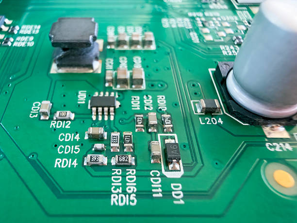
For RF and high-speed applications, impedance control is one of the most important manufacturing requirements.
The following factors can influence impedance values:
- Dielectric thickness
- Copper thickness
- Trace width
- Copper roughness
- Material dielectric constant
During production, manufacturers use advanced monitoring methods to maintain consistent impedance performance.
Regular calibration of manufacturing equipment, including LDI systems and inspection tools, helps reduce process variation.
Reliable PCB Manufacturing Services ensure accurate fabrication processes for demanding high-frequency and high-speed electronic applications.
Rogers materials usually have smoother surfaces than conventional PCB materials, which creates additional challenges for copper adhesion.
Before copper plating, manufacturers may apply specialized surface preparation methods to improve bonding strength.
Typical processes include:
- Controlled micro-etching
- Surface activation
- Chemical cleaning
Proper surface preparation helps prevent:
- Copper peeling
- Plating defects
- Reliability failures during operation
High-frequency PCB manufacturing requires strict cleanliness management.
Dust, oil contamination, or foreign particles can negatively affect:
- Lamination quality
- Copper adhesion
- Electrical performance
During manufacturing, special attention should be given to:
- Material handling
- Layer stacking
- Cleanroom control
- Operator protection procedures
Vacuum handling equipment is often used during multilayer assembly to reduce contamination caused by manual contact.
Due to their excellent electrical performance, Rogers-based PCBs are widely used in industries requiring reliable high-frequency signal transmission.
Typical applications include:
5G infrastructure requires PCBs with low signal loss and stable dielectric performance.
Rogers materials are commonly used in:
- Base station antennas
- RF modules
- Communication equipment
Satellite communication systems operate under demanding environmental conditions and require highly reliable RF circuits.
High-frequency Rogers PCBs provide:
- Stable electrical performance
- Low transmission loss
- High thermal reliability
Modern radar systems, especially automotive millimeter-wave radar, require precise signal control.
Rogers PCB technology supports:
- High-frequency operation
- Accurate signal transmission
- Compact RF designs
High-frequency PCB manufacturing requires advanced engineering capability, precise process control, and strict quality management.
gopcba provides professional PCB and PCBA manufacturing solutions for customers worldwide, supporting applications from prototype development to production manufacturing.
The company offers integrated services including:
- High-frequency PCB fabrication
- PCB assembly
- Component sourcing
- Functional testing
- Customized manufacturing solutions
With experienced engineering teams and advanced production capabilities, gopcba helps customers achieve reliable electronic products with optimized performance and shorter development cycles.
Whether developing communication equipment, industrial electronics, medical systems, or advanced RF applications, gopcba provides complete manufacturing support from PCB design verification to final assembly.
The manufacturing process of High Frequency Rogers PCB requires precise control over material selection, circuit fabrication, lamination, drilling, surface finishing, and testing.
Compared with standard FR4 PCBs, Rogers-based circuit boards demand more advanced manufacturing techniques because high-frequency signals are highly sensitive to material and process variations.
By controlling impedance accuracy, maintaining material compatibility, improving surface treatment quality, and implementing strict inspection procedures, manufacturers can ensure reliable performance for demanding RF applications.
As electronic products continue moving toward higher frequencies and faster data transmission, advanced RF PCB Fabrication technology will remain essential for next-generation communication, aerospace, automotive, and industrial systems.
gopcba delivers comprehensive PCB and PCBA manufacturing solutions to support customers requiring high-performance circuit boards with consistent quality, reliability, and scalability.
