High-Precision Multilayer PCB Manufacturing Process: A Complete Guide
What Is a High-Precision Multilayer PCB?
A High-Precision Multilayer PCB is a printed circuit board consisting of multiple conductive layers separated by insulating dielectric materials. Compared with conventional two-layer or simple multilayer boards, high-precision designs require tighter control of layer registration, hole positioning, copper thickness, impedance, dimensional stability, and surface finish.
These PCBs are widely used in applications where electrical performance and reliability are critical, including telecommunications, industrial control, medical electronics, automotive electronics, computing equipment, and other high-density electronic systems.
For these applications, Multilayer PCB Manufacturing is not simply a matter of stacking several copper layers together. Every stage—from material selection and inner-layer imaging to drilling, plating, lamination, and final inspection—must be carefully controlled to maintain electrical continuity and mechanical stability.
For projects requiring controlled manufacturing from prototype through production, professional PCB Manufacturing capabilities can help ensure that the fabrication process matches the electrical and mechanical requirements of the final product.
Key Requirements for High-Precision Multilayer PCB Manufacturing
The most important objectives in high-precision multilayer production include:
- Accurate layer-to-layer registration
- Precise hole positioning and diameter control
- Consistent copper thickness
- Reliable interlayer electrical connections
- Stable lamination dimensions
- Controlled dielectric thickness
- High-quality surface finishing
- Reliable electrical and physical inspection
Among these requirements, PCB Layer Alignment is particularly important. Even a small registration error can affect via connections, trace spacing, impedance performance, and solder-pad positioning.
The manufacturing process therefore needs to combine suitable materials, precision equipment, controlled process parameters, and inspection procedures.
Step 1: Material Selection and Engineering Verification
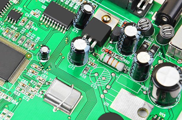
High-precision PCB fabrication begins before production equipment is started. The engineering team first reviews the design requirements and selects materials appropriate for the intended application.
Selecting the PCB Base Material
The laminate should provide suitable:
- Thermal stability
- Dielectric performance
- Dimensional stability
- Mechanical strength
- Moisture resistance
- Copper adhesion
For high-speed or high-frequency applications, dielectric properties become especially important because variations in dielectric constant and dielectric thickness can affect signal integrity and controlled impedance.
Copper Foil Selection
Copper foil thickness must match the electrical and current-carrying requirements of the design.
Important characteristics include:
- Copper thickness
- Surface profile
- Electrical conductivity
- Surface cleanliness
- Adhesion performance
Uniform copper thickness helps maintain predictable trace resistance and improves the consistency of subsequent plating processes.
Prepreg Selection
Prepreg provides insulation and bonding between PCB layers during lamination.
Its resin content, thickness, flow characteristics, and curing behavior need to be compatible with the layer stack-up. Incorrect material selection can lead to excessive resin flow, insufficient bonding, voids, or dimensional deformation.
Step 2: Confirm the PCB Stack-Up and Manufacturing Parameters
Before fabrication begins, the complete stack-up should be reviewed and approved.
Important parameters include:
- Number of PCB layers
- Core thickness
- Copper thickness
- Prepreg configuration
- Finished board thickness
- Via structure
- Trace and spacing requirements
- Controlled impedance requirements
- Surface finish
- Solder mask
- Board dimensions
- Manufacturing tolerances
For complex multilayer boards, the stack-up should be designed together with the electrical requirements rather than treated as an independent manufacturing decision.
A well-defined stack-up helps control dielectric thickness, signal impedance, copper distribution, thermal behavior, and overall board flatness.
Step 3: Inner-Layer Preparation and Circuit Pattern Formation
The inner layers form the electrical foundation of a multilayer PCB.
The copper surface is first cleaned to remove contaminants, oxidation, and other residues. Proper surface preparation improves the consistency of subsequent imaging and etching processes.
The circuit pattern is then transferred onto the copper surface using a controlled imaging process.
After imaging, the unwanted copper is removed through etching, leaving the required circuit traces and copper features.
Why Inner-Layer Accuracy Matters
Inner-layer defects can become difficult or impossible to correct after lamination. Typical problems include:
- Incomplete circuit patterns
- Over-etching
- Under-etching
- Trace width variation
- Copper contamination
- Surface scratches
- Registration errors
Automated optical inspection can be used to detect pattern defects before the inner layers are laminated into the final multilayer structure.
Step 4: Precision Drilling
Drilling creates the physical pathways required for electrical connections between PCB layers.
Depending on the board structure, manufacturers may use mechanical drilling, laser drilling, or a combination of both.
Mechanical Drilling
Mechanical drilling is commonly used for standard through-holes and larger-diameter holes.
High-speed CNC drilling systems can control:
- Hole coordinates
- Hole diameter
- Drilling depth
- Tool condition
- Hole-to-hole spacing
Tool wear must also be monitored because a worn drill can produce dimensional variation, burrs, poor hole-wall quality, or positional errors.
Laser Drilling
Laser drilling is particularly useful for small microvias and high-density interconnect structures.
Laser technology allows manufacturers to create very small openings with controlled depth, making it suitable for advanced multilayer and HDI designs.
The drilling method should be selected according to the via structure, material combination, hole size, and layer configuration.
Step 5: Desmear and Hole-Wall Preparation
After drilling, resin residue and other contaminants may remain inside the holes.
A desmear process removes unwanted resin from the hole walls and prepares the surface for copper deposition.
This step is particularly important because reliable copper plating depends on good adhesion between the hole wall and the deposited copper.
Poor hole-wall preparation may result in:
- Weak copper adhesion
- Voids
- Open circuits
- Poor plating coverage
- Reliability failures during thermal cycling
Step 6: Electroless Copper and Copper Electroplating
Copper plating establishes the conductive connection between PCB layers.
Electroless Copper
Because the drilled laminate is electrically insulating, a thin conductive copper layer is first deposited onto the hole walls through a chemical process.
This creates the conductive foundation required for subsequent electroplating.
Process control should focus on:
- Chemical concentration
- Bath temperature
- Processing time
- Surface activation
- Hole-wall coverage
- Copper adhesion
Copper Electroplating
Electroplating then increases the copper thickness to the required level.
For high-precision boards, current density, plating time, solution circulation, and bath chemistry must be carefully controlled.
Uniform plating is essential because insufficient copper in the hole barrel can reduce current-carrying capability and long-term reliability.
The finished copper thickness should therefore be verified using appropriate thickness measurement and cross-sectional inspection methods.
Step 7: Multilayer PCB Lamination
Lamination is one of the most critical stages of Multilayer PCB Fabrication.
During this process, inner-layer cores and prepreg materials are stacked according to the approved stack-up and bonded together under controlled temperature and pressure.
Layer Stack-Up
Each inner-layer circuit is positioned according to the engineering documentation.
Alignment pins, tooling holes, optical registration systems, or other registration technologies can be used to maintain accurate positioning.
The objective is to ensure that:
- Inner-layer circuits align correctly
- Vias connect to their intended targets
- Dielectric thickness remains within specification
- The finished board remains dimensionally stable
Temperature and Pressure Control
During lamination, prepreg resin softens and flows before curing.
The lamination profile must be carefully controlled to achieve appropriate resin flow and bonding without creating excessive deformation.
Important variables include:
- Temperature ramp rate
- Pressure
- Vacuum
- Pressing time
- Resin flow
- Cooling rate
Poor control may cause delamination, voids, excessive resin flow, warpage, or layer misregistration.
Step 8: Outer-Layer Circuit Fabrication
After lamination, the outer copper layers are processed to form the final external circuitry.
The process may include:
- Surface cleaning
- Pattern imaging
- Copper plating
- Tin plating or another protective process
- Etching
- Stripping
- Inspection
At this stage, trace width, spacing, pad dimensions, and copper distribution must remain within the design requirements.
For high-density boards, even small dimensional deviations can affect component assembly and signal performance.
Step 9: Solder Mask and Surface Finish
The solder mask protects exposed copper areas and helps prevent unintended solder bridges during assembly.
The typical process includes:
- Solder mask coating
- Pre-curing
- Exposure
- Development
- Final curing
The solder mask should provide consistent coverage while keeping component pads and other required exposed copper areas clean and accurately defined.
Surface Finish Selection
A suitable surface finish is selected according to the PCB’s electrical, mechanical, and assembly requirements.
Common options include:
- ENIG
- HASL
- OSP
- Immersion tin
- Immersion silver
For fine-pitch components and applications requiring a relatively flat pad surface, ENIG is often considered because it provides a suitable surface for component soldering and protects the underlying copper from oxidation.
The appropriate finish should ultimately be selected based on the component package, assembly process, reliability requirements, and cost considerations.
Step 10: PCB Quality Inspection and Testing
A comprehensive PCB Quality Inspection program is essential for high-precision multilayer boards.
Inspection should cover both electrical and physical characteristics.
Electrical Testing
Electrical testing can identify:
- Open circuits
- Short circuits
- Incorrect connections
- Insulation failures
- Connectivity problems
Flying-probe testing may be suitable for prototypes and smaller production quantities, while dedicated fixtures can provide efficient testing for larger production volumes.
Automated Optical Inspection
AOI systems inspect circuit patterns and can detect defects such as:
- Missing copper
- Excess copper
- Trace abnormalities
- Pad defects
- Pattern deviations
AOI provides an important inspection layer before the board proceeds to later manufacturing stages.
X-Ray Inspection
X-ray inspection can be useful for examining internal structures that cannot be directly observed from the PCB surface.
It can help evaluate:
- Internal vias
- Layer structures
- Hidden connections
- Voids
- Registration conditions
Cross-Section Analysis
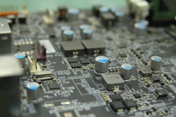
Cross-sectional analysis provides a direct view of the internal PCB structure.
It can be used to verify:
- Copper thickness
- Hole-wall plating
- Layer alignment
- Dielectric thickness
- Lamination quality
- Via structure
For demanding multilayer applications, cross-section analysis is an important tool for process verification and reliability control.
High-Precision PCB Manufacturing Quality Control
A reliable manufacturing system should not depend solely on final inspection. Quality needs to be controlled throughout the entire production process.
A typical quality-control framework includes:
| Manufacturing Stage | Key Control Items |
|---|---|
| Material preparation | Laminate, copper foil, prepreg specifications |
| Inner-layer fabrication | Trace width, spacing, pattern defects |
| Drilling | Hole diameter, position, depth |
| Desmear | Hole-wall cleanliness and preparation |
| Copper plating | Copper thickness and coverage |
| Lamination | Layer registration, thickness, bonding |
| Outer-layer fabrication | Circuit dimensions and defects |
| Solder mask | Coverage, alignment, curing |
| Surface finish | Thickness, uniformity, solderability |
| Final inspection | Electrical, dimensional, visual, reliability testing |
This process-based approach helps identify potential defects before they become embedded in later manufacturing stages.
Design Considerations for High-Precision Multilayer PCBs
Manufacturing performance is strongly influenced by PCB design.
Before releasing a design for production, engineers should review:
Layer Stack-Up
The layer structure should consider signal integrity, power distribution, thermal performance, and mechanical requirements.
Via Design
Via diameter, pad size, aspect ratio, spacing, and connection targets should be compatible with the manufacturing process.
Trace and Spacing
High-density designs require realistic trace-width and spacing rules that match the selected fabrication capability.
Copper Distribution
Uneven copper distribution can contribute to plating variation, thermal imbalance, and board deformation. Balanced copper distribution should therefore be considered during layout.
Thermal and Mechanical Stability
The PCB material, copper distribution, layer structure, and lamination design all influence dimensional stability and resistance to warpage.
For designs that require engineering support before fabrication, PCB Design and Layout services can help evaluate manufacturability and production requirements before the design enters fabrication.
Prototype to Volume Production
The manufacturing strategy may change depending on production volume.
Prototype production generally emphasizes flexibility, rapid engineering verification, and design iteration. Low-volume production requires consistent quality while maintaining manufacturing efficiency. High-volume production places greater emphasis on process repeatability, automation, yield, and cost control.
For early-stage product development, Prototype PCB Assembly can help bridge the gap between PCB fabrication and functional product validation.
When production demand increases, a structured transition toward High Volume PCB Assembly can provide a more scalable manufacturing approach.
How to Improve Multilayer PCB Manufacturing Yield
Several strategies can improve manufacturing consistency and yield:
- Select materials according to the actual application requirements.
- Validate the stack-up before production.
- Use appropriate drilling technology for different via structures.
- Control layer registration throughout lamination.
- Maintain stable plating chemistry and current density.
- Monitor equipment and tooling conditions.
- Use AOI and electrical testing to identify defects early.
- Perform cross-sectional analysis for critical structures.
- Design PCBs according to realistic manufacturing capabilities.
- Track process data to identify recurring sources of defects.
The goal is not simply to inspect defective boards at the end of production, but to prevent defects from occurring in the first place.
Conclusion
The production of a High-Precision Multilayer PCB is a tightly controlled manufacturing process involving material selection, inner-layer fabrication, precision drilling, desmear, copper plating, lamination, outer-layer processing, solder mask, surface finishing, and comprehensive inspection.
Among these processes, PCB Layer Alignment, dimensional stability, hole-wall plating quality, and copper thickness control have a direct impact on the electrical and mechanical reliability of the finished board.
A well-controlled Multilayer PCB Manufacturing process combines engineering verification, appropriate equipment, stable production parameters, and comprehensive PCB Quality Inspection. When these elements work together, manufacturers can achieve more consistent multilayer PCB performance for demanding applications ranging from communications and industrial electronics to medical, automotive, and computing systems.
For projects requiring integrated manufacturing and assembly support, Gopcba provides PCB manufacturing and assembly solutions designed to support product development from prototype quantities through larger-scale production.