As electronic systems become faster, smaller, and more highly integrated, High-Speed PCB Design has become an essential part of modern electronic engineering. High-speed design is not determined simply by the nominal frequency of a digital signal. In many cases, the signal rise time, interconnect length, propagation delay, and electrical behavior of the transmission path are more important.
A system may contain both relatively slow digital interfaces and very fast signals with short edge rates. Even when the clock frequency appears moderate, fast signal transitions can generate significant high-frequency components. Once the interconnect becomes electrically long, transmission-line effects such as reflections, crosstalk, ringing, and impedance discontinuities can no longer be ignored.
For this reason, High-Speed PCB development requires coordinated control of the PCB stackup, routing, reference planes, impedance, power distribution, grounding, and manufacturing tolerances.
What Is High-Speed PCB Design?
High-Speed PCB Design refers to the design of printed circuit boards that carry signals whose electrical behavior is significantly affected by transmission-line effects.
The boundary between high-speed and low-speed design is not fixed. Instead of relying solely on signal frequency, engineers should consider factors such as:
- Signal rise and fall time
- Interconnect length
- Propagation delay
- Transmission-line impedance
- Signal amplitude
- Receiver sensitivity
- Driver output characteristics
- Crosstalk
- Return-current paths
- Power distribution
- Electromagnetic interference (EMI)
High-speed digital systems may include interfaces such as PCIe, USB, DDR memory, Ethernet, SerDes, high-speed ADC/DAC connections, and other differential or single-ended interfaces.
Modern embedded systems and IoT products may also combine high-speed digital circuits with wireless communication and RF front ends. This makes careful partitioning and electromagnetic compatibility an important part of the overall PCB Design process.
Planning the PCB Stackup for High-Speed Design
The PCB Stackup determines much more than the number of copper layers. It directly affects impedance, routing density, signal return paths, power distribution, electromagnetic coupling, and manufacturability.
A well-designed stackup normally provides appropriate signal layers together with continuous reference planes for high-speed routing.
Several factors should be considered when planning the stackup.
Board Size and Number of Nets
The physical dimensions of the board and the number of electrical nets determine the available routing space.
A larger board may provide more routing area, while a compact product may require additional signal layers to accommodate dense interconnects.
However, simply adding layers does not automatically solve routing problems. The stackup should be developed together with the routing strategy, component placement, via structure, and manufacturing capabilities.
Routing Density
High component density can significantly reduce the routing space available on outer layers.
When routing density becomes high, additional internal signal layers may be required. Designers should also consider via placement, escape routing, differential-pair requirements, and layer transitions when estimating the required number of layers.
Interface Distribution
High-speed interfaces should be assigned carefully to appropriate routing layers.
Keeping related signals within the same layer or layer group can help maintain consistent geometry and impedance. Differential pairs should also be routed with controlled spacing and a stable reference structure.
For buses with strict timing requirements, length matching and skew control may be necessary.
Low-Speed and RF Signals
A complex board may contain high-speed digital, low-speed control, analog, and RF circuits simultaneously.
These signals should not simply be routed according to available space. Their electromagnetic relationships should be considered during stackup and floorplanning.
Sensitive analog or RF circuits may require physical separation from noisy digital interfaces, while high-speed digital signals should have controlled return-current paths.
Power Integrity and Ground-Plane Planning
Power distribution is a fundamental part of High-Speed PCB performance.
Large integrated circuits can generate rapid changes in current demand. If the power distribution network has excessive inductance or impedance, these current transients can produce voltage fluctuations and power-supply noise.
A robust power-distribution structure generally includes:
- Appropriate power planes or copper regions
- Continuous ground reference planes
- Properly selected decoupling capacitors
- Short connections between capacitors and device power/ground pins
- Low-inductance current paths
- Carefully designed power distribution networks
Power and ground planes are often placed on adjacent layers where appropriate to create a low-inductance power distribution structure. However, the exact stackup should be optimized according to the device requirements and the PCB’s overall geometry.
Impedance Control in High-Speed PCB Design
Impedance Control is one of the most important elements of high-speed interconnect design.
Common controlled-impedance targets include 50 Ω single-ended and 90–100 Ω differential interfaces, although the actual target depends on the interface specification and system architecture. Other impedance values can also be required for specific applications.
For example, a design may contain 27 Ω, 33 Ω, 75 Ω, or 120 Ω differential structures. Therefore, engineers should never assume that every high-speed signal requires the same impedance.
Multiple impedance targets can exist within the same PCB.
This means the required trace width and spacing may vary between routing structures. The final values should be calculated using the actual PCB stackup and material properties rather than applying a universal trace-width rule.
What Determines PCB Trace Impedance?
The impedance of a PCB transmission line depends on several physical parameters, including:
- Trace width
- Copper thickness
- Distance to the reference plane
- Dielectric thickness
- Dielectric constant (Dk)
- Trace geometry
- Copper surface profile
- Differential-pair spacing
- Manufacturing tolerances
For microstrip structures, the relationship between the trace and the adjacent reference plane is particularly important.
For stripline structures, the signal is embedded between reference planes, which can provide better electromagnetic confinement and more predictable impedance.
Therefore, PCB Stackup planning and Impedance Control should be performed together.
High-Speed PCB Routing Guidelines
1. Establish a Routing Strategy Before Routing
Before starting detailed PCB Routing, designers should determine:
- Critical signal groups
- Reference layers
- Differential-pair requirements
- Target impedance
- Length-matching requirements
- Maximum allowable vias
- Layer-transition strategy
- Sensitive analog and RF regions
- Power and ground structures
Critical signals should generally be routed first, followed by less-sensitive interfaces.
Automatic routing can be useful for certain non-critical connections, but critical high-speed nets usually require carefully controlled interactive routing.
2. Minimize Unnecessary Layer Transitions
Every via introduces a discontinuity into the signal path.
For high-speed signals, excessive vias can increase parasitic effects and may create undesirable via stubs. Where appropriate, designers should minimize unnecessary layer transitions.
If a high-speed signal must change layers, the return-current path should also be considered. A nearby ground via may help provide a low-inductance transition for the return current when the reference structure changes.
3. Control Differential-Pair Geometry
Differential signals depend on the electrical relationship between the two traces.
The pair should generally be routed with controlled width and spacing, while maintaining a consistent reference environment.
Abrupt changes in spacing, unnecessary routing detours, large via structures, and discontinuities can introduce differential skew and impedance variation.
For high-speed differential interfaces, both intra-pair matching and the overall routing environment should be evaluated.
4. Avoid Long Parallel Routing
Long parallel traces can increase capacitive and inductive coupling between neighboring signals.
This can cause crosstalk, particularly when aggressive edge rates are involved.
Designers should therefore avoid unnecessarily long parallel runs between sensitive and noisy signals. Where sufficient spacing cannot be maintained, changes in routing layer, ground shielding structures, or other appropriate isolation techniques may be considered.
The correct spacing should be determined according to the stackup, signal characteristics, and interface requirements rather than a single universal spacing rule.
Grounding and Return-Current Paths
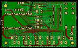
Grounding is not simply a matter of connecting every ground point together. In High-Speed PCB Design, the path taken by return current is extremely important.
A high-frequency signal tends to follow a return path that minimizes impedance, often concentrating around the reference plane beneath the signal trace.
If a signal crosses a split plane, large gap, or other discontinuity in its reference structure, the return current may be forced to take a longer path.
This can increase loop area and potentially cause:
- Higher electromagnetic radiation
- Increased inductance
- Signal distortion
- Crosstalk
- EMI problems
For this reason, maintaining continuous reference planes beneath critical high-speed signals is often preferable.
Digital and Analog Grounding
A common design mistake is to assume that digital and analog grounds must always be physically separated.
The correct strategy depends on the system architecture.
For many mixed-signal designs, maintaining a continuous and carefully managed ground plane can provide a better return-current path than creating unnecessary ground splits.
Instead of automatically separating grounds, engineers should focus on:
- Current-return paths
- Physical placement
- Noise sources
- Sensitive circuits
- ADC/DAC interfaces
- Power distribution
- Clock routing
- Connector locations
Where a specific converter, RF device, or system architecture requires special grounding treatment, the manufacturer’s reference design and system-level EMC requirements should be followed.
Power and Ground Routing
When routing resources are limited, designers should avoid compromising critical reference planes simply to gain additional routing space.
A solid ground reference is particularly valuable for high-speed signals.
Power routing should also be designed according to expected current, voltage drop, thermal requirements, and transient behavior.
Rather than using fixed universal trace widths, the required width should be calculated based on current, copper thickness, allowable temperature rise, voltage drop, and manufacturing constraints.
Large Copper Areas and Thermal Relief
Large copper areas can provide electrical and thermal benefits, but they can also influence soldering behavior.
When a component pad is connected directly to a large copper area, the copper can act as a significant heat sink during soldering.
Thermal relief structures can reduce heat loss from the pad and help improve solderability in appropriate applications.
However, thermal relief should be selected according to the component type, current requirement, thermal performance, and manufacturing process.
For high-current connections, a solid copper connection may sometimes be preferable to thermal relief. The correct design therefore depends on the electrical and manufacturing requirements.
PCB Grid and Layout Planning
A consistent layout grid can simplify component placement and routing.
Traditional PCB design environments commonly use grid-based placement to improve alignment and reduce unnecessary routing complexity.
However, modern high-density PCB design should not be restricted to a single fixed grid value. Fine-pitch components and advanced packages may require smaller placement and routing increments.
The grid should therefore be selected according to:
- Component pitch
- Package geometry
- Manufacturing capability
- Routing density
- Design-rule requirements
The objective is to maintain an organized layout without unnecessarily restricting the routing solution.
Design Rule Checking
Design Rule Checking (DRC) is an essential step in the PCB Design process.
A complete DRC review should check more than simple clearance violations. Depending on the project, the review may include:
- Minimum trace width
- Minimum spacing
- Via dimensions
- Hole-to-copper clearance
- Differential-pair spacing
- Length constraints
- Impedance requirements
- Power and ground clearances
- Component spacing
- Manufacturing limitations
For high-speed interfaces, electrical constraints should also be reviewed using appropriate simulation and analysis tools.
Simulation Before and After Routing
Simulation can significantly improve the reliability of a High-Speed PCB design.
Before routing, engineers can use simulation to estimate acceptable ranges for:
- Trace impedance
- Termination values
- Signal rise time
- Propagation delay
- Crosstalk
- Via structures
- Length matching
- Power-distribution behavior
After routing, the actual PCB topology can be evaluated to determine whether the implemented design meets the required electrical performance.
This pre-layout and post-layout approach is particularly valuable for high-speed interfaces with strict signal-integrity requirements.
Signal Integrity and Termination
Signal Integrity (SI) is a central consideration in high-speed design.
When a signal travels through a transmission line, impedance discontinuities can produce reflections. These reflections may appear as ringing, overshoot, undershoot, or timing errors at the receiver.
Depending on the interface, termination techniques may include:
- Source termination
- Parallel termination
- Thevenin termination
- Differential termination
- AC termination
The appropriate method depends on the driver, receiver, transmission-line impedance, signal topology, voltage level, and interface specification.
Termination should therefore be selected based on simulation and the device manufacturer’s recommendations rather than applying one method to every high-speed net.
Choosing the Right Driver Technology
The signal driver should match the electrical requirements of the system.
Important parameters include:
- Rise and fall time
- Output impedance
- Signal amplitude
- Load capacitance
- Noise margin
- Receiver characteristics
- Transmission-line impedance
An unnecessarily fast driver can increase EMI and ringing without providing a meaningful system-level benefit.
In some applications, controlling the edge rate can improve electromagnetic compatibility and signal quality.
PCB Manufacturing Considerations
A theoretically excellent high-speed design can still fail if it cannot be manufactured consistently.
PCB Manufacturing tolerances directly affect impedance.
Variations in dielectric thickness, copper thickness, trace width, etching, resin distribution, and material Dk can change the final impedance.
For controlled-impedance boards, designers and manufacturers should therefore define realistic fabrication tolerances during the engineering stage.
This is one reason why stackup design should be developed in cooperation with the PCB manufacturer.
At Kingda, high-speed PCB projects can be evaluated from both design and manufacturing perspectives, helping engineers consider stackup construction, impedance requirements, routing constraints, material selection, and production tolerances before fabrication.
Key Considerations for High-Speed PCB Design
A successful High-Speed PCB Design process can be summarized into several major principles:
- Define the electrical requirements before routing.
- Build an appropriate PCB Stackup around the required impedance and reference planes.
- Maintain stable signal return-current paths.
- Control trace geometry and differential-pair spacing.
- Minimize unnecessary vias and via stubs.
- Reduce long parallel routing between sensitive signals.
- Design power distribution and decoupling carefully.
- Use simulation to validate critical interfaces.
- Apply DRC and manufacturing constraints throughout the design process.
- Verify the final design against actual PCB Manufacturing capabilities.
Conclusion
Modern High-Speed PCB Design is a system-level engineering process rather than simply a matter of routing shorter traces.
As data rates increase and electronic systems become more integrated, Impedance Control, Signal Integrity, power integrity, return-current management, and manufacturing consistency become increasingly important.
A carefully planned PCB Stackup, controlled routing geometry, stable reference planes, appropriate termination, and simulation-based verification can significantly improve high-speed system performance.
At the same time, designers should avoid relying on fixed universal rules for trace width, grounding, spacing, or termination. The correct solution depends on the interface, materials, stackup, component characteristics, and manufacturing process.
By combining sound PCB Design principles with SI/PI simulation, DRC, and close coordination with the PCB manufacturer, engineers can create high-speed boards that deliver reliable electrical performance while maintaining manufacturability and production consistency.