High Speed PCB Versus Ordinary PCB: Where The Difference Shows
The difference between a high speed board and an ordinary one is not a single feature but a set of decisions that ripple through the design, the material selection and the manufacturing process. An ordinary PCB is designed to make the circuit work, and the interconnect is assumed to be transparent. A high speed PCB is designed on the understanding that the interconnect is part of the circuit, and that assumption changes almost everything downstream.
This article compares the two across the areas where the difference actually shows up, and it also describes when the additional work is not worth doing.
The comparison matters practically, because the cost of a high speed board comes from a handful of specific choices, and knowing which ones are needed keeps a design from paying for controls it does not use.
Design Intent
An ordinary board is laid out to realise a schematic. Traces connect pins, the routing is short where it can be and the designer’s attention is mostly on correctness, clearances and manufacturability. Signal integrity, in the sense of waveform quality, is rarely a factor, because the interconnections are short enough that the signals arrive essentially as they left.
A high speed board is laid out with the electrical behaviour of the interconnect in mind. The impedance of each critical net is a design parameter, the length of the nets relative to each other is controlled, the reference plane is continuous beneath every controlled line, and the return current has a planned path. Those requirements come from the multilayer structure that high speed boards rely on.

Material Selection
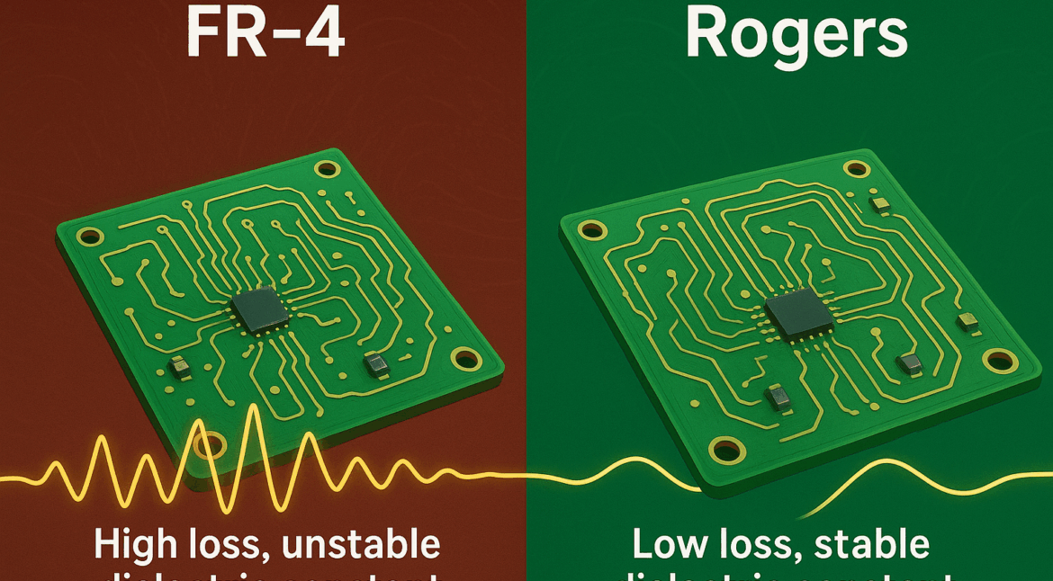
An ordinary board is usually built on standard FR-4, and the copper weight is chosen for the current it has to carry. The laminate is treated as an insulator rather than as part of the signal path, so its dielectric constant and its loss factor are not considered.
A high speed board may use the same material for most of its layers and a lower loss laminate for the ones carrying the fastest signals, which is a common and economical compromise. What differs is that the material is chosen deliberately, with the dielectric constant specified tightly enough that the impedance control is meaningful and with the loss factor considered for the longest or fastest routes.
Impedance Control And The Stackup
Impedance control is the clearest dividing line. An ordinary board has no impedance target, so the trace width is whatever the design rules produce. A high speed board specifies a target per layer and a tolerance, and the stackup is calculated to support it, with the dielectric thickness between each signal layer and its reference plane chosen rather than inherited.
That calculation is shared with the fabricator, who recalculates the line widths for the material actually used and verifies the result by measurement. The consequence is that the stackup becomes a controlled document, and the review of the artwork against it becomes a step in the process rather than a formality.
Vias And Layer Transitions
An ordinary board uses through vias, which are simple, cheap and completely adequate where the signal path is not electrically critical. A high speed board may need more. A through via leaves an unused length of barrel, and that stub becomes a resonant structure at high frequency, so a controlled impedance transition requires either back drilling to remove it or a blind via that stops at the target layer.
Those options cost money because they add process steps and reduce yield, and the decision to use them should follow from the rise time of the signals involved. A board that uses blind vias where a through via would do is paying for manufacturing difficulty without gaining performance.
Fabrication And Surface Finish
Manufacturing tolerances differ as well. A high speed board requires tighter control of line width, more consistent lamination, and impedance verification on a coupon. The surface finish is chosen with the assembly and the frequency in mind, since a flat finish with uniform properties supports both a consistent launch and a reliable solder joint. The process window is narrower at every step, which is why the same geometry can cost noticeably more when it is specified as controlled impedance.
Electrical testing is also more extensive. An ordinary board is tested for continuity and isolation, while a high speed board may also be measured for impedance and inspected for the quality of the plating inside the vias that carry the signal.
Performance Consequences
The results are visible in the numbers a high speed design is judged by: the insertion loss of a channel, the return loss at a connector, the width of the opening in an eye diagram and the margin against crosstalk. An ordinary board built on the same geometry would show a larger reflection at every transition, more attenuation at the top of the band and a narrower margin.
How much of that matters depends on the interface. A general purpose microcontroller board at modest speed does not benefit from a controlled stackup, and adding one only increases the cost. The judgment to be made is whether the edges in the design and the lengths of the routes put the interconnect into the region where its behaviour matters.
When Ordinary Is Good Enough
Most boards are ordinary boards, and that is the correct outcome. Where the traces are short compared with the rise time of the signals, where the interfaces run at modest rates, and where the supplies and the ground structure are sound, a conventional design works and is cheaper to build and easier to debug.
The high speed approach becomes necessary when a signal has to travel far enough, or changes fast enough, that the interconnect is no longer transparent. At that point the controls described above stop being optional, and the design has to be treated as a transmission line problem rather than a wiring problem. gopcb builds both kinds of board, and will advise on which controls a particular design actually needs rather than applying the most demanding specification by default.
Process Control and Verification
On a design of this kind, signal integrity is the item that decides how the rest of the board is arranged. The measurements that matter are the repeatable ones: conductor width and spacing, annular ring, finished hole size, plating thickness and surface finish are all verifiable on a coupon that travels with the panel. Running a first article through the same checks as the production panel confirms that the two agree, and that comparison is the cheapest form of process control available at prototype stage.
FAQ
Is a high speed PCB simply a board with a fast processor on it? No. What matters is the behaviour of the interconnect, which depends on the rise time of the signals and the length of the routes rather than on the processor alone.
Do I have to use a special laminate? Only where the loss or the dielectric constant tolerance of ordinary FR-4 is not good enough. Many high speed designs use improved FR-4 for most layers.
Are blind vias always required? No. They are used where a via stub would degrade the signal. Where a through via is short enough not to resonate in the band of interest, it remains the cheaper choice.