How Are PCBs Manufactured? A Complete PCB Manufacturing Process Guide
How Are PCBs Manufactured?
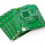
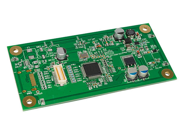
A printed circuit board (PCB) is the structural and electrical foundation of many electronic products. But how are PCBs manufactured from raw materials into finished circuit boards?
The PCB Manufacturing Process combines material preparation, circuit pattern formation, drilling, copper plating, lamination, solder mask application, surface finishing, inspection, and electrical testing. Each stage must be carefully controlled because a defect introduced early in the process can affect subsequent manufacturing operations and the reliability of the finished board.
The exact process varies according to PCB construction. A simple two-layer board has a relatively straightforward production flow, while multilayer, HDI, high-frequency, rigid-flex, and other advanced PCBs require additional processes and tighter dimensional control.
For a complete overview of professional fabrication capabilities, PCB Manufacturing provides the foundation for understanding how design data is converted into production-ready circuit boards.
Step 1: Material Preparation and Panel Cutting
PCB production begins with selecting the appropriate laminate according to the electrical, thermal, mechanical, and dimensional requirements of the design.
Common PCB materials include FR-4 and specialized high-frequency or high-temperature laminates. The selected material typically consists of a dielectric substrate with copper foil bonded to one or both sides.
The laminate is then cut into production panels according to the required board dimensions and manufacturing layout.
This stage establishes the physical foundation for all subsequent processes. Accurate panel dimensions are important because dimensional errors can affect registration, drilling, routing, and final board geometry.
Step 2: Inner-Layer Circuit Fabrication
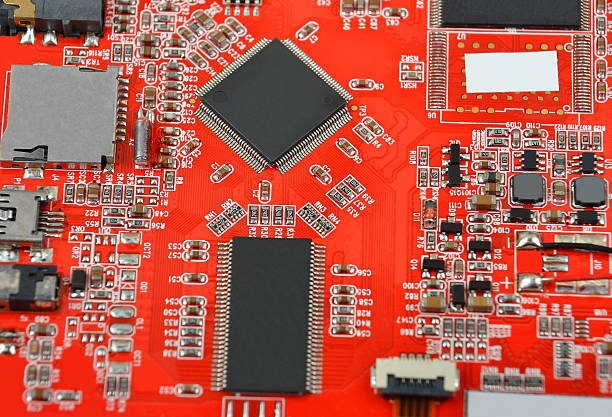
For multilayer PCBs, inner-layer circuit fabrication is one of the most important early stages.
Dry Film Lamination
A photosensitive dry film is laminated onto the copper surface. The film acts as a temporary imaging layer that determines which areas of copper will remain during subsequent etching.
The surface must be properly prepared before lamination to ensure good adhesion and minimize defects.
Inner-Layer Exposure
The circuit artwork is transferred to the dry film using controlled exposure. The exposed areas undergo a chemical change that allows the desired circuit pattern to be developed.
Accurate imaging is essential for maintaining trace width, spacing, pad geometry, and other design features.
Development
The panel is processed through a developing solution that removes the appropriate portions of the dry film and reveals the copper areas that need to be etched.
At this point, the intended inner-layer circuit pattern has been defined on the copper surface.
Inner-Layer Etching
The exposed copper is chemically removed, leaving the designed circuit traces and pads.
Etching must be carefully controlled because excessive or insufficient etching can change conductor dimensions and affect electrical performance.
AOI Inspection
Automated optical inspection (AOI) is used to inspect the inner-layer circuitry.
The inspection system can compare the manufactured pattern with reference data and identify potential defects such as:
- Open circuits
- Short circuits
- Missing copper
- Excess copper
- Pattern deviations
- Incorrect features
Early inspection helps prevent defective inner layers from entering the lamination stage.
Brown Oxide or Bond Enhancement
Before multilayer lamination, the inner-layer copper surface is treated to improve adhesion between the copper and dielectric materials.
This process helps create a stronger interface during lamination and contributes to the mechanical reliability of the finished multilayer PCB.
Step 3: Multilayer Lamination
After the inner layers have been fabricated and inspected, they are stacked together with dielectric materials such as prepreg according to the specified layer stack-up.
The stack is subjected to controlled heat and pressure.
During lamination, the prepreg softens and flows, filling the spaces between layers before curing into a solid insulating structure. This bonds the individual layers into a single multilayer PCB.
Proper control of temperature, pressure, heating rate, and material properties is essential.
Poor lamination can lead to problems such as:
- Delamination
- Voids
- Layer misregistration
- Resin-related defects
- Dimensional instability
- Internal reliability problems
For designs with demanding layer structures, professional PCB Design and Layout planning can help ensure that the stack-up and manufacturing requirements are compatible.
Step 4: Drilling and Hole Formation
Once the multilayer structure has been laminated, holes are drilled according to the manufacturing data.
Drilling creates the openings required for:
- Through-hole components
- Plated through holes
- Vias
- Mechanical mounting
- Tooling and alignment
CNC drilling equipment is commonly used for mechanical holes, while laser drilling may be used for certain microvia structures in advanced HDI designs.
Drill accuracy is critical because the holes must align with pads and internal copper features across multiple layers.
After drilling, the hole walls may contain resin smear and other residues. These contaminants need to be removed before copper plating so that reliable electrical connections can be established.
Step 5: Desmear and Hole Preparation
Drilling can produce resin residue on hole walls, particularly where the drill passes through dielectric material.
A desmear process removes unwanted resin residue and prepares the hole walls for subsequent metallization.
Depending on the board construction and manufacturing requirements, additional chemical or plasma-based processes may be used to improve hole-wall condition.
The objective is to create a clean and properly prepared surface for copper deposition.
Step 6: Electroless Copper and Copper Plating
The drilled hole walls are initially non-conductive because they pass through insulating dielectric material.
Electroless copper deposition creates a thin conductive layer on the hole walls and other required surfaces.
Electrolytic copper plating then increases the copper thickness to achieve the required electrical and mechanical performance.
This stage is particularly important for plated through holes and vias because the copper barrel must provide a reliable connection between different conductive layers.
Plating parameters need to be controlled carefully to maintain uniform copper thickness and adequate coverage throughout the board.
Step 7: Outer-Layer Circuit Formation
After hole metallization, the outer copper layers are processed to form the final external circuit pattern.
The general sequence may include:
- Dry film lamination
- Outer-layer exposure
- Development
- Pattern plating
- Tin or another etch-resistant protective layer
- Dry film stripping
- Copper etching
- Removal of the protective plating
- AOI inspection
The objective is to retain the designed copper features while removing unwanted copper.
Outer-layer imaging and etching require precise process control, particularly for boards with fine traces and narrow spacing.
Step 8: Solder Mask Application
After the circuit pattern has been completed and inspected, solder mask is applied to protect most of the copper surface.
Solder mask provides several important functions:
- Prevents unintended solder bridging
- Protects copper from environmental exposure
- Provides electrical insulation between exposed conductors
- Improves the visual appearance of the PCB
The solder mask is typically applied across the board and then selectively exposed and developed to create openings over pads and other areas that must remain accessible for soldering.
After curing, the solder mask becomes a durable protective layer.
Inspection is then performed to identify issues such as incomplete coverage, misalignment, scratches, contamination, or incorrect openings.
Step 9: Silkscreen and Component Markings
Silkscreen is used to print reference information and markings on the PCB.
Typical markings may include:
- Component reference designators
- Polarity indicators
- Connector labels
- Test-point identifiers
- Product information
- Assembly instructions
Accurate silkscreen positioning is important because markings should remain readable without interfering with component pads or soldering areas.
The printed ink is cured to improve adhesion and durability.
Step 10: Surface Finishing
The exposed copper pads require an appropriate surface finish to protect the copper and provide a suitable soldering surface.
Depending on the application, PCB manufacturers may use different surface finishes, including:
ENIG
Electroless nickel immersion gold (ENIG) provides a relatively flat surface and good solderability. It is commonly used for fine-pitch components and applications where surface flatness is important.
HASL
Hot air solder leveling applies solder to exposed copper and removes excess material using heated air. Lead-free HASL is widely used where lead-free manufacturing is required.
Immersion Tin
Immersion tin provides a relatively flat solderable surface and can be suitable for specific assembly requirements.
Immersion Silver
Immersion silver offers a flat surface and good solderability, making it useful for certain fine-pitch applications.
OSP
Organic solderability preservative (OSP) protects exposed copper while maintaining a suitable surface for soldering.
Hard Gold or Edge Plating
Gold plating can be used for specific contact areas such as connector fingers where wear resistance and electrical contact performance are important.
The appropriate finish depends on assembly technology, storage requirements, contact applications, reliability targets, and cost considerations.
Step 11: PCB Electrical Testing
After fabrication, electrical testing verifies whether the finished PCB satisfies the required electrical connections.
Testing may include:
- Continuity testing
- Isolation testing
- Open-circuit detection
- Short-circuit detection
- Net verification
Electrical testing is particularly important for complex boards containing large numbers of connections.
Testing requirements should correspond to the design data and manufacturing specifications so that the inspection process can accurately determine whether a board is acceptable.
Step 12: Final Routing, Milling, and Dimensional Processing
The production panel is separated into individual boards through routing, milling, punching, or other specified mechanical processes.
The final board outline must match the engineering drawing and mechanical requirements.
Depending on the design, manufacturers may also process:
- Slots
- Cutouts
- Edge connectors
- Mounting holes
- V-grooves
- Countersinks
- Special board profiles
Dimensional accuracy is important because PCB geometry must match the enclosure and mechanical assembly of the finished electronic product.
Step 13: Final Inspection and Quality Control
The final stage is comprehensive inspection before packaging and shipment.
PCB Quality Control may include visual inspection, dimensional measurement, AOI verification, electrical testing, and additional reliability checks according to project requirements.
Typical inspection items include:
| Inspection Item | Purpose |
|---|---|
| Visual Inspection | Identify surface and appearance defects |
| AOI | Verify circuit pattern accuracy |
| Electrical Testing | Detect opens and shorts |
| Dimensional Inspection | Verify board size and geometry |
| Hole Inspection | Check hole size and position |
| Cross-Section Analysis | Evaluate internal structures |
| Surface Finish Inspection | Verify surface treatment quality |
| Solder Mask Inspection | Check coverage and pad openings |
For demanding applications, additional testing may be required to evaluate thermal, mechanical, electrical, or environmental reliability.
How PCB Manufacturing Quality Is Controlled
Quality cannot be added only at the end of production. It needs to be built into every manufacturing stage.
A robust manufacturing workflow typically combines:
- Incoming material inspection
- Engineering data review
- Process parameter control
- In-process inspection
- AOI
- Electrical testing
- Dimensional verification
- Final quality inspection
- Production traceability
This approach allows manufacturers to identify problems as early as possible instead of relying exclusively on final inspection.
PCB Manufacturing for Prototypes and Production
The manufacturing process can be adapted according to the product development stage.
Prototype PCB Manufacturing
Prototype production is used to validate circuit performance, mechanical fit, manufacturability, and assembly processes.
During prototyping, engineering teams may identify issues that require PCB layout or manufacturing revisions. A flexible prototype workflow can therefore shorten development cycles.
Prototype PCB Assembly can be integrated with PCB fabrication when customers need to validate both the bare board and assembled electronics.
Low-Volume Manufacturing
Low-volume production is useful for pilot runs, engineering validation, specialized products, and early market production.
At this stage, maintaining consistent manufacturing documentation and process control is important because design revisions may continue to occur.
High-Volume Manufacturing
Once a design has been validated, production can transition toward larger quantities.
High-volume manufacturing emphasizes repeatability, process stability, yield, production efficiency, and consistent quality.
Integrated High Volume PCB Assembly can support the transition from validated PCB designs to repeatable electronic production.
What Determines PCB Manufacturing Cost?
The cost of manufacturing a PCB depends on several technical and commercial factors.
Important variables include:
- Number of layers
- Board dimensions
- Material selection
- Copper thickness
- Trace and spacing requirements
- Number and type of drilled holes
- Via structures
- Surface finish
- Solder mask requirements
- Special processes
- Testing requirements
- Production quantity
- Manufacturing lead time
More complex boards generally require additional processes, tighter process control, and more extensive inspection.
For this reason, optimizing the design for manufacturability before production can help reduce unnecessary manufacturing costs without compromising required performance.
Why a Controlled PCB Manufacturing Process Matters
Every stage of PCB production affects the stages that follow it. An error during material preparation can affect dimensional accuracy. Poor inner-layer registration can create multilayer connectivity problems. Inadequate drilling or plating can compromise vias and plated through holes. Incorrect solder mask or surface finishing can affect assembly quality.
A controlled PCB Manufacturing Process therefore depends on the combination of accurate production data, appropriate materials, stable equipment, skilled engineering, controlled process parameters, and systematic inspection.
The result is not simply a circuit board that matches the original artwork, but a reliable physical platform capable of supporting the electrical and mechanical requirements of the finished product.
Conclusion
So, How Are PCBs Manufactured?
A typical PCB manufacturing flow starts with material selection and panel cutting, followed by inner-layer circuit fabrication, inspection, lamination, drilling, desmear, copper plating, outer-layer pattern formation, solder mask, silkscreen, surface finishing, electrical testing, final routing, and comprehensive inspection.
While the basic principles remain consistent, the actual process becomes more demanding as PCB designs move toward higher layer counts, finer geometries, advanced via structures, specialized materials, and tighter electrical requirements.
For reliable PCB production, each manufacturing stage must be carefully coordinated and supported by accurate design data and systematic PCB Quality Control. This process-oriented approach helps manufacturers produce circuit boards with consistent electrical performance, dimensional accuracy, assembly compatibility, and long-term reliability.