How Does a PCB Work? PCB Design & PCB Manufacturing Guide
At first glance, a Printed Circuit Board (PCB) may look like nothing more than a flat board covered with copper traces and miniature components. However, a closer look reveals that a PCB is a carefully engineered electrical and mechanical system that provides the foundation for modern electronic products.
PCBs are found in smartphones, computers, automotive systems, industrial equipment, medical devices, communication systems, consumer electronics, and countless other applications. Although their shapes, materials, layer counts, and functions can vary significantly, their fundamental purpose remains similar: to provide a structured platform for electrically and mechanically connecting electronic components.
So, how does a PCB work?
A PCB itself does not normally process information in the way a microprocessor does. Instead, it provides the conductive paths, power distribution, grounding structure, mechanical support, and interconnections that allow components to form a functional electronic circuit. Components such as resistors, capacitors, transistors, integrated circuits, sensors, and connectors work together according to the circuit design.
This article explains the structure of a PCB and how its different parts work together to deliver the required electrical functions.
What Is a PCB?
A PCB is a board that mechanically supports electronic components and electrically connects them through conductive patterns.
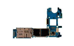
Depending on circuit complexity and product requirements, PCBs can be classified as:
- Single-sided PCBs
- Double-sided PCBs
- Multilayer PCBs
- Rigid PCBs
- Flexible PCBs
- Rigid-flex PCBs
- HDI PCBs
- Specialized high-frequency or high-power PCBs
The electrical behavior of a PCB is determined by its schematic, component characteristics, routing, layer stackup, power distribution, grounding, and other design parameters.
During PCB Design, engineers determine how components should be interconnected and how signals and power should travel through the board. During PCB Manufacturing, these electrical requirements are converted into physical copper structures, dielectric layers, vias, solder mask, and other PCB features.
PCB Structure
A PCB consists of multiple materials and structures that work together. Although the exact construction varies according to the application, most PCBs include several fundamental elements.
1. PCB Substrate
The substrate provides the mechanical foundation of the PCB.
For many rigid PCBs, FR-4 is commonly used. FR-4 is a glass-fiber-reinforced epoxy laminate that provides a combination of mechanical strength, electrical insulation, thermal performance, and manufacturability.
Other applications may use different materials.
For example:
- Polyimide is widely used for flexible circuits.
- Aluminum substrates are used in many thermal-management applications.
- Ceramic substrates can be used for high-temperature or high-frequency applications.
- Specialized laminates are used for RF, microwave, and high-speed applications.
The substrate is not simply a mechanical support. Its dielectric properties can directly influence signal integrity, impedance, capacitance, and high-frequency performance.
2. Copper Layers
Copper is the primary conductive material used in most PCBs.
Depending on the board configuration, copper may be present on one side, both sides, or multiple internal layers.
The copper is patterned to create:
- Traces
- Pads
- Planes
- Vias
- Power distribution structures
- Ground connections
During PCB fabrication, unwanted copper is removed or otherwise separated from the required conductive pattern.
Trace width and copper thickness must be selected according to electrical current, voltage drop, thermal requirements, impedance, manufacturing capability, and other design constraints.
In multilayer PCBs, copper layers are separated by dielectric materials and interconnected using vias.
3. Solder Mask
The Solder Mask is a protective insulating coating applied over much of the PCB surface.
The familiar green appearance of many PCBs comes from the solder mask, although other colors such as black, blue, red, white, and yellow are also available.
Solder mask helps:
- Protect exposed copper
- Reduce the risk of accidental solder bridges
- Protect the board from environmental contamination
- Improve electrical insulation
- Define areas where solder should and should not be applied
The solder mask does not itself carry electrical signals. Instead, it protects and electrically isolates much of the underlying copper.
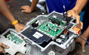
4. Electronic Components
Electronic components provide the actual electrical functions implemented by the PCB.
Components may include:
- Resistors
- Capacitors
- Inductors
- Diodes
- Transistors
- Integrated circuits
- Microcontrollers
- Microprocessors
- Memory devices
- Sensors
- Relays
- Connectors
Components can be broadly classified as active or passive.
Active components can control, amplify, switch, process, or otherwise modify electrical signals. Passive components generally perform functions such as resistance, capacitance, inductance, filtering, energy storage, or signal conditioning.
Components can also be classified according to their mounting method:
- Through-Hole Technology (THT) components
- Surface-Mount Technology (SMT) components
The components are connected to PCB pads or plated holes through soldered joints.
5. Holes and Vias
Holes and vias provide mechanical and electrical connections within a PCB.
Through-holes may be used for:
- Through-hole component leads
- Mechanical mounting
- Electrical interconnection
In multilayer PCBs, different via structures are used to connect copper layers.
Common types include:
- Through vias
- Blind vias
- Buried vias
- Microvias
A through via generally extends through the board, while a blind via connects an outer layer to one or more internal layers. A buried via connects internal layers without being directly accessible from the outer surfaces.
These structures allow electrical signals and power to move between different PCB layers.
6. Terminals and Connectors
Connectors provide electrical and mechanical interfaces between the PCB and external systems.
A PCB may contain:
- Power connectors
- Data connectors
- Board-to-board connectors
- Cable connectors
- Test connectors
- Antenna connections
- External I/O interfaces
Through these interfaces, a PCB can receive power and external signals and transmit processed signals or control outputs to other devices.
7. Silkscreen
The PCB Silkscreen is a printed identification layer used to display information on the board.
It may include:
- Component reference designators
- Polarity indicators
- Pin-1 markings
- Connector labels
- Test-point identifiers
- Manufacturer information
- Warning symbols
- Assembly instructions
Silkscreen does not normally perform an electrical function. Instead, it supports PCB assembly, inspection, troubleshooting, and maintenance.
How Does a PCB Work?
The fundamental operation of a PCB comes from the interaction between the circuit components and the conductive structures that connect them.
The PCB provides the physical infrastructure, while the components perform specific electrical functions according to the schematic.
The basic process can be understood through several key concepts.
Electrical Connectivity
Copper traces act as conductive paths between components.
When power is applied to a circuit, current flows through the designed electrical network according to the circuit topology and component characteristics.
For example, a power trace may carry current from a connector to a voltage regulator. The regulator then provides an appropriate voltage to a microcontroller or other circuit block.
Ground planes and return paths provide corresponding paths for current to return to the power source.
Therefore, PCB operation is not simply about making traces connect. The physical layout of those traces, planes, vias, and reference structures can significantly affect electrical performance.
Signal Routing
A PCB also provides paths for electrical signals.
For example, a sensor may generate an analog signal that travels through a PCB trace to an amplifier or analog-to-digital converter. A digital interface may transfer data between a microcontroller and memory device through multiple signal traces.
In high-speed designs, engineers must carefully control:
- Trace impedance
- Trace length
- Differential-pair geometry
- Return paths
- Crosstalk
- Via transitions
- Reference planes
This is why PCB Layout is an essential part of modern PCB engineering.
Component Response
Each component interacts with electrical signals according to its physical characteristics.
For example:
- A resistor limits current and creates voltage drops.
- A capacitor stores electrical charge and can filter or couple signals.
- An inductor stores energy in a magnetic field and can filter or regulate current.
- A diode primarily allows current to flow preferentially in one direction and can provide rectification or protection.
- A transistor can function as a switch or amplifier.
- A microcontroller executes programmed instructions and controls other circuit functions.
- A voltage regulator converts an input voltage into a controlled output voltage.
The PCB connects these components so that their individual functions combine into the desired system behavior.
Power Distribution
Power distribution is another fundamental aspect of how a PCB works.
A typical PCB may receive power from an external connector, battery, or power supply. The power then passes through protection and regulation circuits before being distributed to individual functional blocks.
A power-management section may include:
- Voltage regulators
- DC-DC converters
- Linear regulators
- Protection devices
- Filtering capacitors
- Inductors
- Current-sensing circuits
The PCB layout must provide sufficiently low-resistance and low-inductance paths where required.
High-current PCB designs may require wider traces, larger copper areas, thicker copper, multiple vias, or dedicated power planes.
Grounding and Return Paths
Ground is not simply an unused copper area. It provides a reference potential and, depending on the circuit, an important return path for current.
A well-designed ground structure can help reduce:
- Noise
- Voltage fluctuations
- Ground potential differences
- Electromagnetic interference
- Signal-integrity problems
Multilayer PCBs often use dedicated ground planes to provide controlled and low-impedance return paths.
Feedback and Control
Many electronic systems use feedback loops to regulate their operation.
For example, a power-management circuit may monitor its output voltage and adjust its switching or control mechanism to maintain the desired output.
Similarly, a temperature-control system may use a sensor to measure temperature and provide feedback to a controller.
The PCB provides the physical interconnections required for these feedback signals to travel between sensors, controllers, and actuators.
Feedback is therefore a function of the overall electronic circuit rather than a function performed by the PCB substrate itself.
A Simple Example of How a PCB Works
Consider a basic embedded control board.
The operating sequence might look like this:
Power Input → Protection → Voltage Regulation → Microcontroller → Signal Processing → Output Interface
A sensor may provide an input signal to the microcontroller. The microcontroller processes the information according to its firmware and then sends an output signal to another circuit.
The PCB connects every part of this system.
For example:
- A power connector supplies the input voltage.
- Protection components protect the circuit against electrical faults.
- A regulator generates the required operating voltage.
- The microcontroller receives power and sensor signals.
- The PCB traces connect the sensor to the appropriate input.
- The microcontroller processes the signal.
- Output signals are routed to a display, motor driver, communication interface, or other circuit.
- Ground and power structures complete the electrical paths.
This example illustrates an important distinction: the PCB provides the physical electrical infrastructure, while the components and firmware determine most of the circuit’s functional behavior.
PCB Design and PCB Manufacturing
Understanding how a PCB works is directly related to both PCB Design and PCB Manufacturing.
During design, engineers determine:
- Circuit architecture
- Component selection
- Component placement
- Routing
- Layer stackup
- Power distribution
- Grounding
- Impedance
- Thermal management
- Manufacturing constraints
During manufacturing, these requirements are converted into a physical board through processes such as:
- Lamination
- Imaging
- Etching
- Drilling
- Plating
- Solder mask application
- Surface finishing
- Silkscreen printing
- Electrical testing
After fabrication, PCB assembly adds the electronic components through SMT, THT, or mixed-technology processes.
The final PCBA therefore combines the fabricated PCB with electronic components to create a functioning electronic assembly.
What Determines PCB Performance?
The performance of a PCB is influenced by much more than the number of components on the board.
Important factors include:
Circuit Architecture
The schematic determines how components interact and what functions the system can perform.
Component Selection
Component specifications directly influence electrical performance, reliability, power consumption, and operating range.
PCB Layout
Placement and routing influence signal integrity, thermal performance, electromagnetic compatibility, and manufacturability.
Materials
The substrate and dielectric materials influence mechanical strength, thermal behavior, dielectric properties, and high-frequency performance.
Copper Structure
Copper thickness, trace width, plane area, and via structures influence current-carrying capability, resistance, voltage drop, and thermal performance.
Manufacturing Quality
Poor drilling, plating, etching, lamination, soldering, or assembly can cause electrical and mechanical failures even when the original design is correct.
Conclusion
A PCB may appear to be a simple board, but it is actually a carefully engineered platform that combines electrical connectivity, mechanical support, power distribution, grounding, signal routing, and component integration.
So, how does a PCB work?
The PCB itself primarily provides the physical and electrical infrastructure that connects the components. Copper traces, planes, pads, and vias create conductive paths, while components such as resistors, capacitors, transistors, ICs, sensors, and processors perform the specific electrical functions defined by the circuit design.
As PCB Design and PCB Manufacturing technologies continue to advance, new approaches such as HDI, flexible and stretchable circuits, embedded components, advanced substrates, and additive manufacturing are expanding what PCBs can achieve.
For engineers and manufacturers such as Kingda, understanding the relationship between circuit architecture, PCB layout, materials, manufacturing processes, and component behavior is essential for developing reliable and high-performance electronic products.