How to Choose Copper Thickness for Heavy Copper PCBs
Copper thickness is one of the most important factors affecting PCB current capacity, thermal performance, reliability, and manufacturing cost. Although copper is only one part of a printed circuit board, its thickness directly influences how much current a conductor can carry, how much heat it generates, and how effectively that heat can be distributed.
A simple way to understand the relationship is to compare copper thickness with the number of lanes on a highway. If the copper is too thin, current capacity may be limited and electrical losses can increase. If the copper is unnecessarily thick, manufacturing becomes more complicated and the PCB cost can rise.
For applications such as renewable energy systems, energy storage, industrial power supplies, motor drives, EV charging equipment, and battery systems, a properly engineered Heavy Copper PCB can provide the current capacity and thermal performance required for demanding operating conditions.
The correct copper thickness should not be selected simply by choosing the thickest available option. Instead, it should be determined by current requirements, allowable temperature rise, trace geometry, board structure, thermal management, manufacturing capability, and cost.
What Copper Thickness Standards Are Used for PCBs?
PCB copper thickness is commonly specified in ounces per square foot, abbreviated as oz. This unit describes the approximate weight of copper distributed over one square foot of board area and is commonly used to indicate copper weight.
Typical conversions are shown below:
| Copper Weight | Approximate Thickness | Typical Applications |
|---|---|---|
| 0.5 oz | 17 μm | High-frequency signal boards and light-load products |
| 1 oz | 35 μm | Consumer electronics and general industrial control |
| 2 oz | 70 μm | Medium-current circuits and power boards |
| 3 oz | 105 μm | High-current control boards and industrial power supplies |
| 6 oz | 210 μm | Energy storage, EV systems, and high-current power applications |
| 10–12 oz | 350–420 μm | Extremely high-current and specialized industrial equipment |
In practical PCB manufacturing, boards using approximately 2 oz or more copper are often considered heavy copper designs, although the exact definition can vary by manufacturer and application.
The actual finished copper thickness may also differ from the starting copper foil thickness because electroplating can add additional copper during fabrication. Therefore, engineering specifications should clearly distinguish between base copper weight and finished copper thickness.
For demanding applications, understanding the relationship between Copper Thickness and the overall PCB stack-up is essential. Copper weight should be evaluated together with trace width, layer count, dielectric thickness, via structure, and thermal requirements.
When Do You Need a Heavy Copper PCB?
Not every power circuit requires heavy copper. A standard 1 oz or 2 oz PCB may be completely adequate for low- and medium-current applications.
A heavy copper design becomes more attractive when one or more of the following conditions apply:
- High current must travel through relatively long PCB traces.
- Power components generate significant localized heat.
- The equipment must operate continuously under high load.
- The operating environment has elevated temperatures.
- Voltage drop must be minimized.
- The PCB requires improved thermal distribution.
- High mechanical robustness is required around power connections.
Typical applications include:
- Industrial power supplies
- Solar inverters and renewable energy systems
- Energy storage equipment
- Electric vehicle charging systems
- Battery management systems
- Motor drives and controllers
- Power distribution equipment
- Railway power electronics
- Specialized aerospace and industrial equipment
For these applications, a High-Current PCB can be engineered with thicker copper, wider conductors, large copper planes, optimized vias, and appropriate thermal structures.
How Does Copper Thickness Affect PCB Performance?
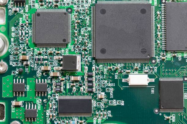
Increasing copper thickness increases the cross-sectional area available for current flow. This can reduce conductor resistance and help control heat generation under high-current conditions.
However, copper thickness alone does not determine current capacity. Trace width, conductor length, allowable temperature rise, ambient temperature, PCB layer structure, airflow, and thermal connection to other components must also be considered.
Higher Current-Carrying Capacity
A thicker copper layer provides a larger conductive cross-sectional area. This allows a PCB trace to carry more current without reaching the same temperature rise as a thinner conductor of comparable geometry.
For high-current circuits, engineers may combine increased copper thickness with wider traces or large copper areas. This approach can improve power distribution while maintaining reasonable temperature levels.
Lower Electrical Resistance
Electrical resistance decreases as conductor cross-sectional area increases. Thicker copper can therefore reduce voltage drop and I²R losses in high-current paths.
Lower resistance can provide several benefits:
- Reduced power loss
- Lower conductor heating
- Improved energy efficiency
- Reduced voltage drop
- Better long-term electrical stability
These advantages are particularly valuable in power conversion, battery systems, motor control, and energy management equipment.
Improved Thermal Performance
High current inevitably creates heat. If the heat cannot be effectively transferred away from the conductor and power components, localized hot spots can develop.
A properly designed Power PCB can use thicker copper together with copper planes, thermal vias, large pads, heat-spreading structures, and appropriate substrate materials to establish a more effective thermal path.
Rather than treating copper thickness as an isolated specification, thermal performance should be evaluated as part of the complete PCB design.
Improved Mechanical Robustness
Thicker copper can also contribute to mechanical robustness in areas such as high-current terminals, connectors, mounting points, and power component connections.
This can be useful in equipment exposed to vibration, mechanical stress, repeated thermal cycling, or demanding industrial environments.
How Much Copper Thickness Should You Choose?
The appropriate copper thickness depends primarily on the electrical and thermal requirements of the actual product.
A general reference can be structured as follows:
| Copper Weight | Approx. Thickness | Typical Use |
|---|---|---|
| 1 oz | 35 μm | General-purpose electronics |
| 2 oz | 70 μm | Moderate-current power circuits |
| 3 oz | 105 μm | High-current industrial and power applications |
| 4 oz | 140 μm | Higher-current power distribution |
| 6 oz | 210 μm | Energy storage and high-power electronics |
| 10 oz+ | 350 μm+ | Specialized high-current applications |
These values should be treated as engineering reference points rather than universal design rules. The correct choice should be validated against the required current, conductor dimensions, temperature-rise target, available board area, and manufacturing process.
For example, increasing copper from 1 oz to 3 oz can substantially improve current-handling capability, but the actual improvement depends on trace width, trace length, ambient temperature, board construction, and cooling conditions.
Similarly, moving from 3 oz to 6 oz does not automatically provide a proportional increase in current capacity. At higher copper weights, trace geometry and manufacturing constraints become increasingly important.
What Happens If You Choose Excessively Thick Copper?
More copper is not always better.
Using unnecessarily thick copper can introduce several disadvantages.
Higher Manufacturing Cost
Thicker copper requires more copper material and may require additional plating and processing time. As copper weight increases, manufacturing costs can therefore rise.
More Difficult Routing
Thick copper can make fine-line fabrication more challenging. The required trace width and spacing may increase depending on the fabrication process and copper thickness.
This can reduce routing flexibility, particularly on compact multilayer boards.
Greater Etching Complexity
Heavy copper requires careful control of the etching process. Excessive lateral etching can affect conductor geometry, while insufficient process control may produce dimensional variation.
The thicker the copper, the more important process optimization becomes.
Longer Production Time
Heavy copper boards may require additional plating, etching, lamination, drilling, and inspection processes. As a result, production lead times can be longer than those of conventional PCBs.
More Difficult Thermal and Mechanical Design
Very thick copper can influence board weight, thermal expansion behavior, stack-up construction, and lamination requirements. These factors should be evaluated during engineering rather than after the design is finalized.
For this reason, professional PCB Manufacturing should balance electrical requirements with manufacturability and overall project cost.
Can Different Copper Thicknesses Be Used on the Same PCB?
Yes. A PCB does not necessarily need to use the same copper thickness on every layer.
Depending on the design, engineers may use different copper weights for external and internal layers. High-current layers can receive thicker copper, while signal layers can use thinner copper.
This approach can reduce unnecessary material usage while maintaining the required electrical performance.
For example, a multilayer power board might use heavier copper on layers carrying high current while maintaining standard copper on signal-routing layers. This can provide a better balance between performance, routing density, manufacturing complexity, and cost.
In some specialized designs, embedded copper structures or copper coins can also be used to provide localized current-carrying or heat-spreading capability.
Heavy Copper PCB Manufacturing Considerations
Heavy copper PCB fabrication requires tighter process control than conventional PCB manufacturing because increased copper thickness affects several manufacturing stages.
Material Selection
FR-4 is widely used for many heavy copper applications. High-Tg materials may be selected when the PCB must withstand higher operating temperatures or demanding thermal conditions.
Material selection should consider:
- Operating temperature
- Thermal expansion
- Dielectric properties
- Mechanical requirements
- Layer count
- Copper thickness
- Long-term reliability
Etching and Plating
Thicker copper requires carefully controlled imaging, etching, and electroplating processes.
The manufacturing process must maintain the specified conductor width and spacing while achieving the required copper thickness. Uniform copper distribution is also important for controlling dimensional stability and board quality.
Lamination
Multilayer heavy copper PCBs require careful lamination engineering. Copper thickness, resin flow, dielectric thickness, layer balance, heating and cooling rates, and registration all influence final board quality.
A properly engineered stack-up can help minimize warpage, delamination, internal voids, and dimensional variation.
Drilling and Via Design
Vias carrying high current require appropriate electrical and thermal design. Depending on the application, engineers may use larger vias, parallel vias, via arrays, or other enhanced structures.
Via construction should be evaluated together with current requirements, PCB thickness, copper plating thickness, thermal resistance, and manufacturing limitations.
How to Optimize Copper Thickness for Cost and Performance
The most cost-effective solution is not necessarily the PCB with the lowest copper weight or the highest copper weight. It is the design that provides sufficient electrical and thermal performance without unnecessary manufacturing complexity.
A practical optimization process can include:
- Determine the maximum continuous and peak current.
- Define the allowable temperature rise.
- Calculate the required conductor cross-sectional area.
- Evaluate trace width and copper thickness together.
- Consider the thermal path from power components.
- Determine whether multilayer copper distribution can improve performance.
- Evaluate via current capacity and thermal requirements.
- Review manufacturing limitations with the PCB supplier.
- Compare standard, heavy copper, and localized copper solutions.
- Validate the final design through prototype testing.
For complex power electronics, early engineering review can prevent excessive copper specifications that increase cost without delivering meaningful performance benefits.
Why Manufacturing Capability Matters
Selecting copper thickness based only on a catalog specification can create problems later in production. The manufacturer’s actual capabilities for etching, plating, lamination, drilling, layer registration, and inspection must also be considered.
A reliable manufacturer should be able to evaluate:
- External and internal copper thickness
- Minimum trace width and spacing
- Board thickness
- Layer count
- Via construction
- Material selection
- Copper distribution
- Surface finish
- Electrical testing
- Thermal requirements
- Production volume
GOPCBA provides customized PCB manufacturing solutions covering heavy copper, multilayer, high-Tg, high-frequency, rigid-flex, HDI, and other advanced PCB technologies. Its manufacturing services can support projects from prototype development through production.
For high-current power applications, heavy copper manufacturing must be considered as a complete process rather than simply a copper-weight specification.
How to Choose the Right Copper Thickness for Your Project
The right copper thickness depends on the combination of electrical load, thermal conditions, PCB dimensions, manufacturing requirements, and budget.
As a starting point:
- 1 oz: Suitable for many standard electronic circuits.
- 2 oz: A practical option for moderate-current power circuits.
- 3 oz: Suitable for many high-current industrial and power applications.
- 4–6 oz: Appropriate when substantially higher current capacity and thermal performance are required.
- 10 oz or more: Generally reserved for specialized high-current applications with demanding electrical and mechanical requirements.
However, these ranges should not replace engineering calculations and manufacturer review.
The best solution may involve thicker copper only on selected layers rather than increasing the copper weight across the entire board.
Conclusion
Copper thickness is a fundamental design parameter for heavy copper and high-current PCBs, but choosing the right value requires more than simply selecting the largest available copper weight.
Current capacity, temperature rise, trace geometry, thermal management, PCB stack-up, via design, material selection, manufacturability, production cost, and long-term reliability must all be evaluated together.
A well-engineered Heavy Copper PCB can provide higher current capacity, lower electrical resistance, improved thermal distribution, and greater reliability for demanding power applications. At the same time, excessive copper thickness can increase cost and manufacturing complexity without necessarily providing proportional performance improvements.
For high-current electronics, the most effective strategy is to select copper thickness according to the actual electrical and thermal requirements of the product, then validate the design with an experienced PCB manufacturing partner.