How to Connect Components on a PCB: PCB Design, PCB Manufacturing & Assembly Guide
Printed circuit boards (PCBs) are the foundation of modern electronic products. They provide the physical platform on which electronic components are mounted and the electrical interconnection structure through which those components communicate and receive power.
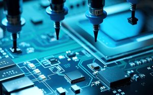
From a technical perspective, a PCB connects electronic components through copper traces, pads, vias, plated holes, and other conductive structures. However, successfully connecting components is not simply a matter of drawing a line between two points. Component packages, footprints, orientation, polarity, electrical ratings, clearance, thermal requirements, and assembly processes must all be considered during PCB Design, PCB Manufacturing, and PCB assembly.
For beginners, understanding how components are connected to a PCB can seem complicated. The process becomes much easier to understand when it is divided into several stages, beginning with circuit design and component selection and continuing through PCB layout, component placement, soldering, inspection, and electrical testing.
This guide explains how to connect components on a PCB and introduces the major technologies and manufacturing steps involved.
What Are the Main PCB Component Mounting Technologies?
As PCB technology has evolved, electronic components have become smaller, more integrated, and more suitable for automated assembly. Two fundamental component mounting technologies are still widely used: Through-Hole Technology (THT) and Surface Mount Technology (SMT).
Through-Hole Components
Through-hole components use leads that pass through holes in the PCB.
During PCB fabrication, the required holes are drilled at precisely defined locations. Depending on the board design, these holes may be plated so that the component leads can form electrical connections with the corresponding copper structures.
Common through-hole components include:
- Large capacitors
- Transformers
- Connectors
- Relays
- Power components
- Mechanical switches
- Components requiring additional mechanical strength
After insertion, the leads can be soldered to the PCB, creating both an electrical and mechanical connection.
Through-hole components are particularly useful when a component needs strong mechanical support or when the application involves relatively high mechanical stress.
Surface-Mount Components
Surface-mount devices (SMDs) are mounted directly onto copper pads on the PCB rather than inserted through drilled component holes.
SMD components are available in many compact packages, including:
- QFN
- QFP
- SOIC
- SOT
- BGA
- 0201, 0402, 0603, and other passive component packages
Because SMD components do not require conventional through-holes for their leads, they can be placed at high density. This makes SMT highly suitable for modern compact electronic products.
During automated assembly, solder paste is deposited onto the PCB pads, components are accurately placed using a pick-and-place machine, and the assembly is passed through a controlled reflow soldering process.
Many modern PCBs use a combination of SMT and THT components depending on electrical, mechanical, thermal, and product requirements.
How to Connect Components on a PCB
The component connection process involves much more than physical mounting. The electrical connection must first be correctly defined in the schematic and PCB layout, followed by accurate component placement, soldering, inspection, and testing.
1. Create the Circuit Design and Prepare the PCB Layout
Every PCB project begins with an electrical design.
Engineers first create a schematic that defines the electrical relationships between components. The schematic establishes which pins are connected, where power is distributed, how signals travel, and how functional blocks interact.
The schematic is then converted into a physical PCB layout.
During this stage, designers need to consider:
- Component package and footprint
- Pin assignments
- Component orientation
- Polarity
- Electrical ratings
- Trace width
- Trace spacing
- Pad dimensions
- Via structures
- Board-layer configuration
- Thermal requirements
- Mechanical clearances
- Manufacturing tolerances
For example, polarized components such as electrolytic capacitors, diodes, LEDs, and certain IC packages require careful attention to orientation. Incorrect polarity can cause malfunction or component damage.
Through-Hole Connections
For THT components, component holes are positioned according to the footprint defined in the PCB layout.
The drilled holes must be correctly aligned with the component leads. Electrical isolation between unrelated nets must also be maintained.
Importantly, not every PCB hole is automatically electrically isolated. A plated through-hole may intentionally connect copper layers or a specific net. Therefore, the electrical purpose of each hole must be defined correctly in the PCB design.
Surface-Mount Connections
For SMD components, copper pads are created according to the component footprint.
Each pad is electrically associated with the appropriate net. The pads must maintain sufficient spacing to prevent unintended solder bridging and electrical shorts.
For fine-pitch components such as BGAs and QFNs, pad geometry, solder-mask design, paste aperture design, and manufacturing tolerances become especially important.
This demonstrates why accurate footprint creation and library management are critical parts of PCB Design.
2. Place Components on the PCB
Once the PCB layout has been prepared, components can be physically placed on the board.
The placement method depends largely on whether the components are THT or SMT.
Through-Hole Component Placement
Through-hole components are commonly inserted into the corresponding holes in the PCB.
In some assembly environments, component leads may be preformed or trimmed to suit the required assembly process. However, lead preparation should follow the component manufacturer’s recommendations and the assembly process requirements rather than using a universal procedure.
During insertion, operators or automated equipment must verify:
- Component reference
- Orientation
- Polarity
- Correct footprint
- Lead position
- Component height
- Mechanical clearance
Correct component orientation is especially important for polarized components and connectors.
Surface-Mount Component Placement
SMD components are generally placed using automated pick-and-place equipment.
The process normally begins with solder paste deposition using a stencil. The solder paste is applied to the appropriate PCB pads.
A pick-and-place machine then:
- Retrieves components from feeders.
- Identifies component type and orientation.
- Moves the component to the programmed PCB location.
- Places the component onto the solder-paste-covered pads.
The accuracy of the placement machine is critical for fine-pitch components and high-density PCB assemblies.
Automated SMT placement is particularly important for volume production because manually placing hundreds or thousands of small components would be inefficient and would introduce unnecessary variability.
3. Solder the Components to the PCB
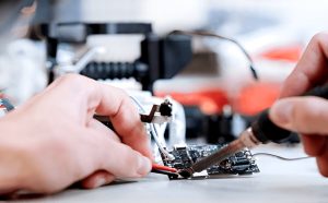
Soldering creates the permanent electrical and mechanical connection between components and the PCB.
Different component technologies require different soldering processes.
Reflow Soldering for SMT
For most SMT assemblies, solder paste is applied to the PCB pads before component placement.
The PCB then passes through a reflow oven with a controlled thermal profile.
A typical reflow process includes several stages:
- Preheating
- Thermal soaking
- Reflow
- Controlled cooling
The solder paste melts during the reflow stage and forms solder joints between the component terminals and PCB pads.
The exact thermal profile depends on factors such as solder alloy, PCB construction, component requirements, and solder-paste manufacturer’s specifications. Therefore, there is no single universal reflow temperature or profile suitable for every PCB assembly.
Wave Soldering for Through-Hole Components
Wave soldering is commonly used for suitable THT assemblies, although selective soldering and other processes may also be used depending on the board design.
After components are inserted, the PCB passes over a controlled wave of molten solder. The solder contacts the exposed leads and corresponding PCB pads, creating solder joints.
Wave soldering is useful for efficiently processing suitable through-hole assemblies, particularly when many THT connections need to be soldered.
For mixed-technology assemblies, manufacturers may use a combination of SMT reflow, THT insertion, selective soldering, wave soldering, and manual soldering where appropriate.
4. Inspect and Verify the Connections
Inspection is a critical part of PCB Manufacturing and assembly because a visually complete board is not necessarily an electrically functional board.
Inspection should be performed throughout the production process rather than only at the very end.
Incoming Material Inspection
Before assembly begins, incoming materials should be checked.
Typical inspection items include:
- PCB specifications
- Board dimensions
- Layer count
- Surface finish
- Component part numbers
- Component quantities
- Package types
- Component condition
- Moisture-sensitive-device requirements
Proper material control helps prevent incorrect components from entering production.
PCB Fabrication Inspection
Bare PCBs should be checked for issues such as:
- Incorrect dimensions
- Drill defects
- Open circuits
- Short circuits
- Damaged pads
- Copper defects
- Solder mask defects
- Surface-finish problems
Depending on the product requirements, manufacturers may use automated optical inspection (AOI), electrical testing, dimensional inspection, microsection analysis, or other quality-control methods.
Component Placement Inspection
After component placement, automated inspection can verify whether components are located and oriented correctly.
AOI can identify issues such as:
- Missing components
- Incorrect components
- Component misalignment
- Polarity errors
- Solder bridging
- Solder-related defects
For assemblies containing hidden solder joints, such as certain BGA packages, X-ray inspection may be required because the solder connections cannot be reliably inspected from the surface.
Solder Joint Inspection
Solder joints should be examined for manufacturing defects.
Potential problems include:
- Insufficient solder
- Excessive solder
- Solder bridges
- Opens
- Component displacement
- Voids where applicable
- Poor wetting
- Cracked or mechanically damaged joints
A dull or unusual appearance alone should not automatically be treated as proof of a defective solder joint. Inspection should consider the applicable solder alloy, process requirements, component type, and accepted workmanship criteria.
5. Perform Electrical and Functional Testing
After assembly, electrical and functional testing helps determine whether the components are actually connected and operating as intended.
Depending on the product, testing may include:
Continuity Testing
Continuity testing verifies whether intended electrical paths are connected.
It can help identify:
- Open circuits
- Broken traces
- Missing connections
- Certain assembly defects
However, continuity alone does not prove that the complete circuit functions correctly.
In-Circuit Testing
In-Circuit Testing (ICT) can evaluate specific electrical characteristics of the assembled PCB and help detect manufacturing-related faults.
ICT may be used to identify:
- Component-value problems
- Open circuits
- Short circuits
- Incorrect component placement
- Certain component failures
Functional Testing
Functional testing evaluates whether the assembled PCB performs its intended system-level functions.
Depending on the application, this may involve checking:
- Supply voltages
- Current consumption
- Digital interfaces
- Analog signals
- Communication protocols
- Sensor outputs
- Motor control
- Display functions
- Protection circuits
For higher-reliability applications, additional testing may be required according to product specifications and applicable industry standards.
Key Points to Remember When Connecting PCB Components
Several important principles should be considered throughout the design and assembly process.
1. Define Components Accurately
Every component should have a correct reference designator, part number, footprint, value, and electrical specification.
A mistake in the component library can propagate through the entire manufacturing process.
2. Pay Attention to Polarity and Orientation
Polarized components must be installed in the correct direction.
This applies to components such as:
- Diodes
- LEDs
- Electrolytic capacitors
- Certain ICs
- Connectors
- Batteries
3. Control ESD and Moisture
Electronic components should be handled and stored according to their requirements.
Electrostatic discharge (ESD) controls are important for sensitive components, while moisture-sensitive devices may require controlled storage and handling according to the applicable moisture-sensitivity requirements.
4. Keep the PCB Clean
Flux residues, particulates, and other contaminants should be controlled according to the assembly process and product requirements.
Not every PCB requires the same cleaning process. Whether cleaning is necessary depends on the flux chemistry, assembly materials, electrical requirements, environmental conditions, and downstream processes such as conformal coating.
5. Manage Heat-Generating Components
Power components and other heat-generating devices require appropriate thermal management.
Designers should consider:
- Copper area
- Thermal vias
- Heat sinks
- Airflow
- Component spacing
- PCB material
- Power dissipation
Thermal design should begin during PCB Design, rather than waiting until the assembly has already been manufactured.
6. Inspect Solder Joints Thoroughly
A reliable solder connection requires appropriate pad design, component placement, solder material, thermal processing, and inspection.
Automated inspection technologies such as AOI and X-ray can be incorporated when appropriate.
7. Test the Completed Assembly
Final testing should verify both electrical connectivity and functional performance.
A successful assembly should not simply look correct; it should meet the specified electrical, mechanical, thermal, and functional requirements.
PCB Design Considerations for Reliable Component Connections
Reliable component connections begin before the first component is physically mounted.
During PCB Design, engineers should establish appropriate design rules for:
- Trace width and spacing
- Pad dimensions
- Via sizes
- Annular rings
- Solder-mask clearance
- Component spacing
- Creepage and clearance
- Thermal relief
- Differential-pair routing
- Controlled impedance
- Power distribution
- Ground return paths
For high-speed circuits, the physical connection between two components can affect signal integrity significantly. Trace length, impedance, return paths, layer transitions, vias, and reference planes should therefore be considered together.
For high-current circuits, the designer must also consider conductor resistance, temperature rise, copper thickness, and current distribution.
In other words, how components are connected on a PCB is determined partly by the physical assembly process and partly by decisions made much earlier in the design stage.
The Relationship Between PCB Manufacturing and PCB Assembly
PCB Manufacturing and PCB assembly are closely related but represent different stages.
PCB Manufacturing produces the bare circuit board. Major processes can include:
- Material preparation
- Inner-layer imaging
- Etching
- Lamination
- Drilling
- Desmear
- Copper plating
- Outer-layer processing
- Solder mask application
- Surface finishing
- Silkscreen
- Routing
- Electrical testing
- Final inspection
PCB assembly then mounts electronic components onto the fabricated board through SMT, THT, soldering, inspection, and testing processes.
The two processes must be designed to work together. For example, the PCB footprint must match the component package, the pad geometry must be suitable for the selected assembly process, and the board’s mechanical dimensions must support the final product.
How Kingda Can Support PCB Assembly
A reliable PCB assembly process requires coordination among PCB designers, component suppliers, PCB manufacturers, and assembly engineers.
Kingda provides integrated PCB and PCBA services, helping customers move from design review and DFM analysis through PCB fabrication, component sourcing, SMT assembly, THT assembly, inspection, and testing.
This integrated approach can be particularly useful for projects involving complex multilayer boards, high-density components, high-speed circuits, HDI structures, rigid-flex PCBs, heavy-copper boards, or other demanding applications.
Early collaboration with the manufacturing and assembly team can help identify footprint, component placement, DFM, DFA, and process-related issues before production begins.
Conclusion
Connecting components on a PCB is one of the most important stages of the PCB assembly process. However, reliable component connections begin long before soldering. They start with accurate schematic design, appropriate component selection, correct footprints, strategic component placement, and carefully planned PCB routing.
During manufacturing and assembly, the correct combination of SMT, THT, reflow soldering, wave or selective soldering, inspection, and electrical testing helps ensure that components are securely and correctly connected.
For engineers and beginners learning PCB Design, the key principle is to think about the complete lifecycle of the board. A component connection must be electrically correct, mechanically reliable, thermally appropriate, and compatible with the intended manufacturing process.
By combining careful design, controlled PCB Manufacturing, accurate assembly, comprehensive inspection, and functional testing, manufacturers can produce PCB assemblies with better reliability, consistency, and long-term performance.
Article Summary
This guide explains how to connect components on a PCB, covering THT and SMT technologies, schematic and PCB layout preparation, component placement, reflow and wave soldering, AOI and X-ray inspection, electrical testing, and key reliability considerations. Proper component connections depend on decisions made throughout the PCB Design, PCB Manufacturing, and PCB assembly processes. Careful planning, accurate component placement, appropriate soldering, and comprehensive testing are essential for producing reliable electronic products.