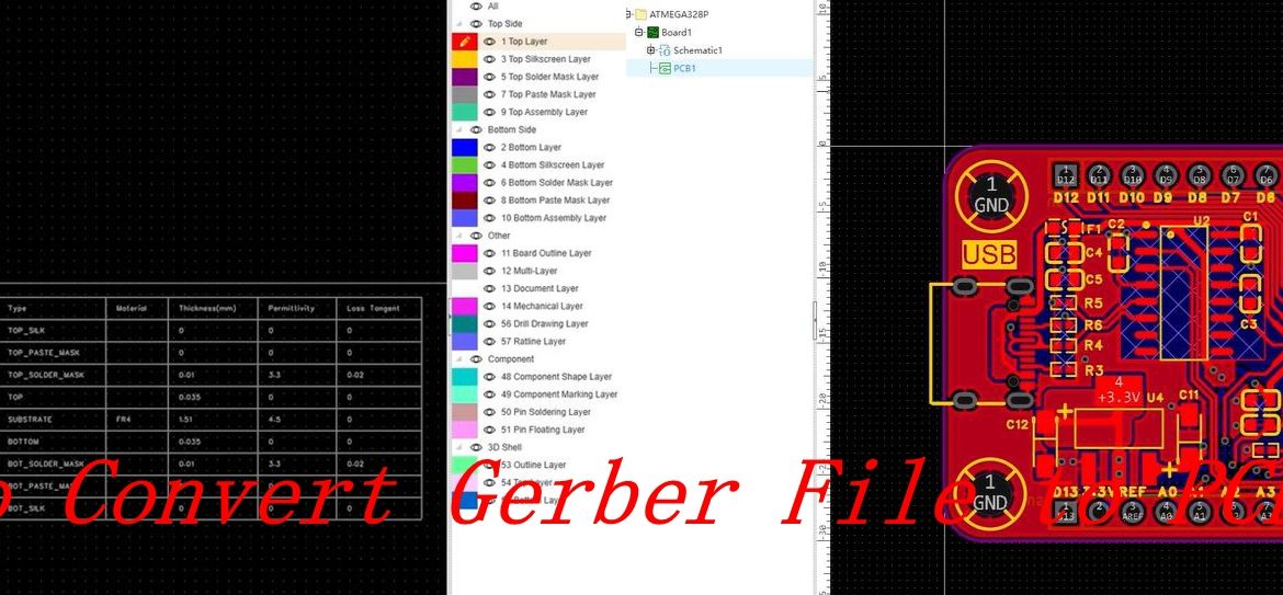
How to Convert Gerber Files to PCB Files: PCB Design & PCB Manufacturing Guide
In electronic engineering, Gerber files are one of the most widely used manufacturing data formats for printed circuit boards. They provide PCB manufacturers with the graphical information required to fabricate the physical board. You can think of Gerber files as a standardized manufacturing language for PCB production, much like source files are used in software development.
But what happens when you need to work in the opposite direction? What if you have Gerber files but no longer have the original editable PCB design files?
This situation is more common than many engineers expect. Original design files can be lost, archived in obsolete software formats, or become unavailable when working with legacy products. In other cases, engineers may need to repair, reproduce, or reverse-engineer an existing PCB based only on its manufacturing data.
Understanding how to convert Gerber files into PCB files can therefore be a valuable skill in PCB Design and PCB Manufacturing. However, it is important to understand that Gerber-to-PCB conversion is generally a reconstruction process rather than a perfect one-click conversion.
This guide explains what Gerber files and PCB files contain, why conversion may be necessary, and how engineers can reconstruct an editable PCB design from available Gerber data.
What Is a Gerber File?
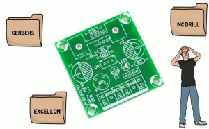
Gerber is a standardized format used to describe the graphical layers required for PCB fabrication. Gerber data can represent copper layers, solder mask, silkscreen, paste layers, and other manufacturing information.
A typical Gerber package may contain separate files for different PCB layers, such as:
- Top copper
- Bottom copper
- Inner copper layers
- Solder mask
- Silkscreen
- Paste layers
- Board outline
Drill information is commonly supplied separately in Excellon or another compatible NC drill format.
Gerber files primarily describe the physical geometry required to manufacture a PCB. They do not normally contain the complete logical design information found in the original PCB project.
Key Characteristics of Gerber Files
1. Two-dimensional manufacturing data
Gerber files primarily contain 2D graphical information representing tracks, pads, regions, openings, and other physical features.
2. Separate data for different layers
A multilayer PCB normally requires multiple Gerber files, with individual files representing different copper, solder mask, silkscreen, and other layers.
3. Manufacturing-oriented information
Gerber files are designed to communicate physical manufacturing information rather than the designer’s complete circuit logic or design intent.
4. No complete schematic or native PCB database
A Gerber package generally does not preserve the original schematic, component relationships, net names, design constraints, or editable component libraries.
This distinction is critical when attempting to convert Gerber data back into a PCB design.
What Is a PCB File?
A PCB file is an editable design file generated by PCB design or EDA software. Depending on the software, it may use formats such as Altium Designer’s .PcbDoc, KiCad’s .kicad_pcb, or other proprietary or open formats.
Unlike Gerber files, a native PCB design file can contain much more than the physical appearance of the board.
Depending on the software and project configuration, a PCB file may contain:
- Component footprints
- Component references
- Copper tracks
- Pads and vias
- Board outline
- Layer information
- Design rules
- Net connectivity
- Component placement
- Routing information
- 3D component models
- Mechanical information
The original PCB project may also be linked to a schematic and component libraries.
This is why converting Gerber files back into a native PCB file is challenging. Gerber data describes the manufactured result, while the original PCB project contains design information and engineering intent that may not be recoverable from the Gerbers alone.
Why Convert Gerber Files to PCB Files?
There are several situations in which engineers may need to reconstruct an editable PCB design from Gerber files.
1. The Original Design Files Are Lost
One of the most common situations is losing access to the original PCB project.
You may still have the manufacturing Gerber package, but the original Altium, KiCad, OrCAD, or other EDA project may no longer be available.
Reconstructing the PCB from Gerber data can provide an editable starting point for future modifications.
2. Working With Legacy PCB Designs
Older products may have been designed using obsolete software or by engineers who are no longer available.
If only manufacturing data remains, converting or reconstructing the design can help engineers maintain, repair, or reproduce the legacy product.
3. Reverse Engineering
Gerber-to-PCB reconstruction can also be part of a reverse-engineering workflow.
Engineers may need to analyze an existing board’s physical layout, reproduce a legacy board, or create a new design based on available manufacturing documentation.
However, reverse engineering should always comply with applicable intellectual-property and contractual requirements.
4. Modifying an Existing Design
Gerber files are excellent for manufacturing but are not convenient for design modifications.
If an engineer needs to change the board outline, routing, component placement, mounting holes, or other design features, reconstructing an editable PCB design can provide a more practical foundation.
How to Convert Gerber Files to PCB Files
Converting Gerber data into an editable PCB project is best understood as PCB design reconstruction.
The exact process depends on the available Gerber files, drill data, EDA software, and the complexity of the original board.
Step 1: Choose Appropriate PCB Design Software
The first step is to select an EDA tool capable of importing or interpreting Gerber data.
Common PCB design platforms and tools include:
- Altium Designer
- KiCad
- OrCAD/Allegro
- EasyEDA
- Dedicated Gerber-to-CAD conversion tools
The software should support the Gerber formats and drill files included in your manufacturing package.
Before beginning, make sure you have a complete data set whenever possible.
Step 2: Import the Gerber Files
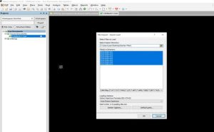
Import all available manufacturing layers into the selected PCB design environment or Gerber viewer/conversion tool.
Typical files may include:
- Top copper
- Bottom copper
- Inner copper layers
- Top solder mask
- Bottom solder mask
- Top silkscreen
- Bottom silkscreen
- Paste layers
- Board outline
- Excellon drill files
Correct layer mapping is extremely important.
For example, accidentally assigning a solder-mask layer as copper can produce an incorrect reconstruction and lead to serious manufacturing problems.
Step 3: Reconstruct the Board Outline
The next step is to establish the physical dimensions and shape of the PCB.
Use the board-outline information from the Gerber package to define:
- Overall board dimensions
- Corners and cutouts
- Mounting holes
- Slots
- Mechanical openings
- Keepout regions
If the original mechanical drawing is available, use it as an additional reference.
Step 4: Reconstruct Pads, Tracks, Vias, and Copper Features
Imported Gerber data can provide the physical geometry of copper features.
Depending on the software, you may need to convert or redraw:
- Pads
- Tracks
- Vias
- Copper pours
- Polygons
- Cutouts
- Other copper features
At this stage, the goal is to reproduce the physical layout as accurately as possible.
Step 5: Reconstruct Component Footprints
Gerber files may show the physical pad patterns and silkscreen information, but they do not necessarily preserve the original component-library relationships.
Engineers may therefore need to recreate or assign component footprints manually.
For each component, verify:
- Pad dimensions
- Pad spacing
- Component orientation
- Reference designator
- Package type
- Pin numbering
- Courtyard or mechanical clearance
If the original BOM is available, it can greatly simplify this step.
Step 6: Reconstruct Net Connectivity
This is one of the most difficult parts of Gerber-to-PCB conversion.
Gerber files generally represent physical copper geometry rather than the logical netlist used during PCB design.
Therefore, the reconstructed PCB may not automatically contain the original net names or component-to-component relationships.
Engineers may need to determine connectivity from:
- Copper traces
- Vias
- Pads
- Component pin assignments
- Available schematics
- BOM information
- Test-point information
- Additional manufacturing documentation
For complex multilayer boards, connectivity reconstruction can require substantial manual work.
Step 7: Recreate Design Rules and Constraints
The original PCB’s design rules are generally not preserved in Gerber files.
You may therefore need to recreate important constraints, including:
- Minimum trace width
- Minimum clearance
- Via dimensions
- Pad-to-copper clearance
- Copper-to-board-edge clearance
- Differential-pair requirements
- Impedance-control requirements
- Layer-specific routing rules
For high-speed or RF designs, this step is particularly important because the physical geometry alone may not reveal all of the original electrical constraints.
Step 8: Verify the Reconstructed PCB
Before using the reconstructed PCB design for manufacturing, perform a comprehensive verification process.
Check the following:
- Board dimensions
- Layer order
- Copper geometry
- Pad positions
- Via locations
- Drill sizes
- Component footprints
- Component orientation
- Track connectivity
- Clearance
- Trace widths
- Solder-mask openings
- Silkscreen placement
- Mounting holes
- Board-edge clearance
Use Design Rule Checking (DRC) where supported.
If possible, compare the reconstructed PCB against the original Gerber package using a Gerber viewer.
Step 9: Generate a Native PCB Project
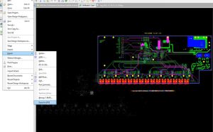
After reconstruction and verification, save the design in the native format supported by your chosen PCB design software.
For example:
- Altium Designer →
.PcbDoc - KiCad →
.kicad_pcb
You should also save the reconstructed schematic, libraries, BOM, design rules, and manufacturing documentation whenever they have been recreated.
Creating a complete project package is much more useful than simply saving a reconstructed board-layout file.
Important Limitations of Gerber-to-PCB Conversion
A critical point is that Gerber-to-PCB conversion is not normally a perfect restoration process.
Gerber files describe the physical manufacturing output, but information from the original design environment may be permanently missing.
The following information may not be recoverable:
- Original schematic
- Original net names
- Component-library links
- Design constraints
- Design intent
- Original component parameters
- Interactive routing information
- Original 3D models
- Engineering notes
- Version history
For this reason, a reconstructed PCB should be carefully verified before it becomes the basis for a new production run.
The more complete the available documentation is, the more accurate and efficient the reconstruction process will be.
Can Gerber Files Be Converted Back to a Schematic?
Generally, no—not directly.
Gerber files describe physical PCB geometry rather than the logical circuit represented by the schematic.
For example, a Gerber file can show that a copper trace connects two physical pads, but it may not tell you the original component names, signal names, circuit functions, or design intent.
A schematic therefore usually needs to be recreated separately using available information such as:
- Existing documentation
- BOM
- Component markings
- Net connectivity
- PCB inspection
- Test measurements
- Original product documentation
For simple boards, schematic reconstruction may be manageable. For complex multilayer boards, it can be a substantial engineering task.
How Accurate Is a Gerber-to-PCB Conversion?
The achievable accuracy depends heavily on the quality and completeness of the source data.
A complete Gerber package containing all copper layers, solder-mask layers, silkscreen layers, board outlines, and drill data provides a much better foundation than an incomplete data set.
Accuracy can also be improved when you have:
- Original BOM
- Component datasheets
- Schematic
- Assembly drawings
- Pick-and-place files
- Mechanical drawings
- Original PCB photographs
- Test-point information
If critical layers or documentation are missing, the reconstructed PCB may not fully represent the original design.
Can a PCB Manufacturer Convert Gerber Files Into PCB Design Files?
PCB manufacturers primarily use Gerber and drill data to fabricate the physical circuit board. They do not normally need the original editable PCB project to manufacture the board.
If you need a native editable PCB design reconstructed from Gerber files, you may need to work with an experienced PCB designer, reverse-engineering service provider, or an engineering team with appropriate EDA tools.
If the reconstructed design will subsequently enter production, the manufacturing partner can then review the new manufacturing files and perform DFM checks before fabrication.
Best Practices for Gerber-to-PCB Reconstruction
To reduce errors and improve the quality of the reconstructed design, follow these practices:
Keep the Complete Gerber Package
Do not work with only the top and bottom copper layers if additional manufacturing files are available. Preserve every available layer and drill file.
Keep the Original Documentation
BOMs, schematics, assembly drawings, mechanical drawings, and photographs can provide valuable information that Gerber files cannot.
Use a Gerber Viewer for Comparison
After reconstruction, compare the new PCB layout with the original Gerber data layer by layer.
Perform DRC and Connectivity Checks
Do not assume that a visually similar board is electrically identical. Check clearances, connectivity, footprints, and manufacturing rules.
Archive the New Project
Once the reconstruction is complete, maintain the native PCB project, schematic, libraries, BOM, design rules, and manufacturing outputs together.
This prevents the same reconstruction problem from occurring in the future.
Conclusion
Converting Gerber files to PCB files is possible, but it should generally be treated as a PCB reconstruction process rather than a simple file-format conversion.
Gerber files provide essential manufacturing information about copper layers, solder mask, silkscreen, board outlines, and drilling. However, they do not normally preserve the complete schematic, netlist, component libraries, design rules, or engineering intent contained in the original PCB project.
By importing the available Gerber and drill data, reconstructing the board geometry, rebuilding footprints and connectivity, recreating design rules, and thoroughly verifying the result, engineers can create a new editable PCB project.
For PCB Design and PCB Manufacturing, maintaining complete source files and manufacturing documentation is always preferable to reconstructing a design later. When original files are unavailable, however, a systematic Gerber-to-PCB workflow can help engineers recover valuable legacy designs, support product maintenance, and prepare boards for future modification or manufacturing.
Kingda can support customers with professional PCB Manufacturing and PCB Assembly services, helping transform verified PCB design data into reliable manufactured circuit boards.