How to Panelize PCBs for SMT Assembly
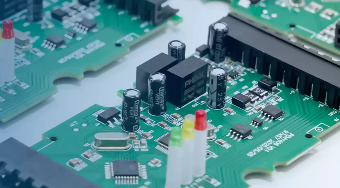
In electronics manufacturing, PCB Panelization is the process of combining multiple individual printed circuit boards into a larger production panel. Panelization allows manufacturers to process several boards at the same time during solder paste printing, component placement, reflow soldering, inspection, and other assembly operations.
For SMT production, a properly designed panel can improve production efficiency, simplify automated handling, reduce setup time, and lower manufacturing costs. It is particularly useful when producing multiple identical boards or when small PCBs would otherwise be inefficient to process individually.
Professional SMT PCB Assembly manufacturers generally review the panel structure, board spacing, tooling edges, fiducial marks, component clearances, and depanelization method before production. A complete manufacturing partner should also consider the relationship between PCB fabrication and assembly requirements.
What Is PCB Panelization for SMT?
PCB panelization combines multiple PCB units into one larger manufacturing panel. The individual boards remain electrically or mechanically connected during fabrication and SMT assembly and are separated after the assembly process.
The main purpose of panelization is to make the PCB easier and more efficient for automated production equipment to handle.
For example, instead of processing ten small PCBs individually, a manufacturer can arrange ten boards into a single panel. The entire panel can then pass through solder paste printing, pick-and-place, reflow, AOI, and other manufacturing processes as one production unit.
This approach is especially beneficial for:
- Small PCB assemblies
- Prototype and low-volume production
- Repetitive PCB designs
- High-volume SMT production
- Multiple boards manufactured in the same production run
- PCB assemblies requiring automated inspection and handling
A professional PCB Assembly manufacturer may also use DFM and DFA reviews to identify panel-related manufacturing risks before production begins.
Why Is PCB Panelization Important for SMT Assembly?
The primary advantage of panelization is improved manufacturing efficiency.
Higher SMT Production Efficiency
Multiple PCBs can be processed during the same machine cycle. This reduces the number of times operators need to load and unload individual boards and helps improve equipment utilization.
Better Automated Handling
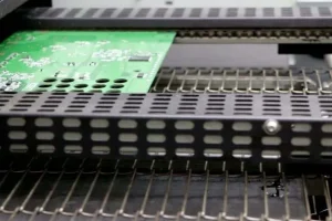
SMT equipment is designed around standardized board handling. A larger and properly supported panel can be easier to transport through solder paste printers, placement machines, reflow ovens, and inspection equipment.
Reduced Production Cost
Panelization can reduce setup and handling operations. It can also make small boards more economical to manufacture because several units can be processed simultaneously.
Improved Production Consistency
Processing multiple boards as one panel helps maintain consistent production conditions across the assembly batch. After assembly, the individual boards are separated using an appropriate depanelization method.
For projects that require both fabrication and assembly, an integrated PCB Manufacturing and assembly workflow can further simplify production coordination.
PCB Panelization Methods for SMT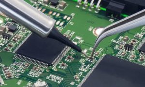
The most common panelization methods include V-cut, routed tabs, and tab-and-hole or stamp-hole structures. The correct method depends on PCB geometry, thickness, component placement, and depanelization requirements.
V-Cut Panelization
V-cut panelization creates a continuous V-shaped groove between adjacent PCB units. After SMT assembly, the boards can be separated along the predefined cutting line.
V-cut is particularly suitable for:
- Rectangular PCBs
- Regular board outlines
- Repetitive PCB designs
- Panels with straight separation lines
Because V-cuts generally require relatively straight separation paths, they are less suitable for highly irregular PCB shapes.
Tab-Routed Panelization
For irregular PCB outlines, routed tabs can be used to connect individual boards to the panel frame.
This method provides greater flexibility for:
- Curved PCB edges
- Irregular board shapes
- Circular or unusual PCB outlines
- Designs requiring customized separation points
The remaining tabs must be strong enough to maintain panel integrity during SMT processing while still allowing reliable depanelization afterward.
Tab-and-Hole or Stamp-Hole Panelization
A series of small holes can be created along the connection area between boards. These structures provide mechanical support while allowing the individual boards to be separated after assembly.
This approach is commonly considered when a simple V-cut cannot accommodate the PCB outline.
How to Design a PCB Panel for SMT
A successful PCB Panel Design should be developed with the entire assembly process in mind rather than simply placing several boards next to each other.
1. Determine the Number of Boards per Panel
Start by determining how many individual PCBs should be included in one panel.
The ideal quantity depends on:
- Individual PCB dimensions
- PCB thickness
- Component density
- SMT machine capability
- Production quantity
- Panel handling requirements
- Depanelization method
Do not simply maximize the number of boards per panel. An excessively large or heavy panel can create handling and warpage problems.
2. Maintain Consistent Board Spacing
Maintain uniform spacing between individual PCB units.
The required clearance depends on the selected manufacturing process, tooling structure, board geometry, and assembly equipment. The spacing should be sufficient to accommodate routing, V-cuts, tabs, tooling, and component clearances.
Consistent spacing also makes the panel easier to inspect and process.
3. Add Tooling Edges
A production panel may require additional tooling or process edges around the PCB array.
Tooling edges provide space for:
- PCB support
- Conveyor handling
- Tooling holes
- Fiducial marks
- Machine positioning
- Automated assembly operations
The required tooling-edge dimensions should be confirmed with your PCB assembly manufacturer before finalizing the panel.
4. Add Fiducial Marks
Fiducial marks are important reference points used by automated SMT equipment to accurately identify panel and PCB positions.
A typical panel may include:
- Global fiducials
- Local fiducials
- Reference marks for individual PCB units
Fiducials should be placed in locations that remain unobstructed and should not be surrounded by copper, solder mask openings, components, or other features that could interfere with optical recognition.
5. Check Component-to-Edge Clearance
Components positioned too close to a PCB edge can interfere with conveyors, fixtures, depanelization tools, or neighboring boards.
Before finalizing the panel, check:
- Component height
- Component orientation
- Component-to-edge distance
- Connector overhang
- Bottom-side components
- Heat-sensitive components
- Depanelization clearance
This is particularly important for connectors, large capacitors, transformers, switches, and other tall or mechanically sensitive components.
6. Keep Board Orientation Consistent
Whenever possible, maintain the same orientation for all identical PCB units.
Consistent orientation simplifies:
- SMT programming
- Component placement
- Inspection
- Manufacturing documentation
- Operator handling
Special arrangements such as rotated boards, mirrored boards, or mixed orientations may be appropriate in certain applications, but they should be evaluated carefully during engineering review.
What Files Are Required for SMT Panelization?
A typical SMT project requires several manufacturing files.
The most important files include:
- Gerber files
- BOM
- Pick-and-place or centroid file
- PCB fabrication drawings
- Assembly drawings
- Special manufacturing instructions
The BOM should clearly identify component part numbers, references, quantities, and other relevant procurement information. Pick-and-place data should accurately correspond with the PCB design and component orientation.
For SMT projects, these files are used to verify the design, prepare the assembly process, program placement equipment, and perform engineering checks.
Should You Panelize the PCB Yourself or Let the Manufacturer Do It?
There are two common approaches.
Customer-Designed Panelization
Experienced PCB designers can create the panel directly in their PCB design software.
This approach gives you maximum control over:
- Board arrangement
- Panel dimensions
- V-cut or routing structure
- Fiducial locations
- Tooling edges
- Depanelization points
However, the completed panel should still be reviewed against the manufacturer’s manufacturing and SMT capabilities.
Manufacturer-Assisted Panelization
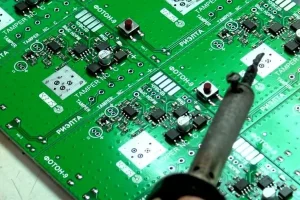
For standard rectangular boards, the manufacturer may be able to create the production panel based on the original PCB design.
This can be useful for customers who do not have extensive panelization experience. The manufacturer can evaluate the board size, component placement, production requirements, and assembly process before preparing the panel.
For more complex boards, professional engineering support is particularly valuable because PCB Assembly involves more than simply duplicating the board outline. Manufacturing data, component placement, tooling, inspection, and depanelization all need to work together.
Common PCB Panelization Problems to Avoid
Several panel design mistakes can lead to manufacturing or assembly problems.
Panel Is Too Large or Too Heavy
An oversized panel can be difficult to transport through SMT equipment and may increase the risk of board warpage.
Components Are Too Close to the Panel Edge
Edge components can collide with tooling, conveyors, neighboring boards, or depanelization equipment.
Insufficient Mechanical Support
A weak connection between individual boards can cause panels to break or deform during transportation and SMT processing.
Fiducials Are Missing or Incorrectly Positioned
Poorly positioned fiducials can make automated optical recognition more difficult and may affect placement accuracy.
Inconsistent Board Spacing
Uneven spacing can complicate routing, tooling, solder paste printing, and depanelization.
Panelization Is Designed Without Considering Depanelization
The way the boards are connected during SMT must be compatible with the way they will eventually be separated. Mechanical stress from depanelization can damage solder joints, ceramic components, connectors, or sensitive PCB structures.
PCB Panelization and Quality Control
Panelization should be included in the engineering and quality-control process rather than treated as a separate cosmetic step.
Before production, the manufacturer should verify the final PCB revision, board specifications, component designators, BOM, pick-and-place data, assembly process, and other special requirements.
During assembly, inspection technologies such as SPI, AOI, X-ray inspection, ICT, and functional testing can be used according to the product requirements. A complete quality workflow can include incoming material inspection, SMT or THT assembly, AOI, X-ray, electrical testing, and final inspection.
PCB Panelization for Prototype and Mass Production
Panelization is not limited to high-volume manufacturing.
For prototypes and low-volume production, a suitable panel can reduce machine setup and handling requirements. For mass production, optimized panel utilization can have an even greater impact on production efficiency and manufacturing cost.
The ideal panel structure may therefore change as a product moves through:
Prototype → Pilot Production → Low-Volume Production → Mass Production
A flexible manufacturing partner should be able to support these different production stages without requiring unnecessary changes to the manufacturing workflow. GOPCBA provides prototype, low-volume, high-volume, turnkey, SMT, through-hole, mixed-technology, and flex PCB assembly services.
How to Start a Panelized SMT PCB Assembly Project
The process can be organized into several practical steps:
- Finalize the individual PCB design.
- Determine the required production quantity.
- Select the appropriate panelization method.
- Define board spacing and tooling edges.
- Add fiducial and tooling features.
- Check component-to-edge clearance.
- Generate the Gerber, BOM, and pick-and-place files.
- Submit the manufacturing data for engineering review.
- Confirm the final panel and assembly process.
- Begin PCB fabrication and SMT assembly.
For a turnkey project, the manufacturer can coordinate PCB fabrication, component sourcing, SMT/THT assembly, inspection, testing, and final delivery as part of one manufacturing workflow.
Final Considerations for PCB Panelization
Good PCB Panelization is not simply about fitting as many boards as possible into a large panel. The panel must be optimized for the complete manufacturing process, including PCB fabrication, solder paste printing, component placement, reflow soldering, inspection, handling, and final depanelization.
When designing a panel, pay particular attention to board spacing, tooling edges, fiducial marks, component clearances, panel rigidity, board orientation, and the selected depanelization method.
If you are looking for a manufacturing partner for SMT PCB Assembly, GOPCBA provides PCB fabrication, SMT, THT, mixed-technology assembly, component procurement, testing, and other PCBA manufacturing services.
For project evaluation, you can submit your Gerber files, BOM, drawings, and other manufacturing information for engineering review and quotation through the company’s contact page.