How to Prepare a PCB for Manufacturing: PCB Design, PCB Manufacturing & DFM Guide
When developing an electronic product, one of the most important elements to consider is the printed circuit board (PCB). A PCB provides both mechanical support and electrical interconnection for electronic components, making proper manufacturing preparation essential for turning an electronic concept into a reliable physical product.
A well-prepared PCB can improve product performance, manufacturing efficiency, reliability, and cost control. In contrast, incomplete design files, incorrect component footprints, insufficient spacing, or missing manufacturing information can result in production delays, rework, unexpected costs, or even complete redesigns.
PCB designs range from simple single-sided boards for basic electronic projects to complex multilayer, HDI, high-speed, and rigid-flex boards used in advanced electronic systems. Regardless of complexity, every PCB should go through a structured preparation process before entering production.
This guide explains how to prepare a PCB for manufacturing, covering schematic design, PCB layout, manufacturing specifications, production files, DFM review, testing requirements, manufacturer selection, and prototype production.
What Is the PCB Manufacturing Preparation Process?
Preparing a PCB for manufacturing is the process of converting an electronic design into a complete, manufacturable set of engineering data.
A typical workflow includes:
- Creating and verifying the schematic
- Designing the PCB layout
- Defining manufacturing specifications
- Preparing manufacturing files
- Performing DFM verification
- Defining testing and programming requirements
- Selecting a PCB manufacturer
- Building and evaluating prototypes
Each stage plays an important role in ensuring that the final PCB can be manufactured accurately and assembled reliably.
1. Create and Verify the Schematic
The schematic is the electrical foundation of the PCB.
Engineers typically use electronic design automation (EDA) software to create a digital representation of the circuit. The schematic defines how components are connected and provides the foundation for the subsequent PCB layout.
Before moving to layout, engineers should carefully verify:
- Component values
- Component symbols
- Pin assignments
- Power connections
- Ground connections
- Net names
- Signal paths
- Connector definitions
- Protection circuits
Electrical Rules Check (ERC) can help identify common schematic errors, such as unconnected pins, invalid connections, or power-related issues.
Simulation may also be appropriate for certain circuits to evaluate electrical behavior before hardware fabrication. Depending on the design, engineers may analyze signal integrity, transient behavior, power integrity, or electromagnetic compatibility concerns.
A clean schematic provides a reliable foundation for the rest of the PCB Design process.
2. Design the PCB Layout
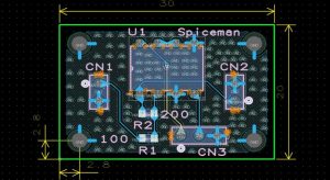
After the schematic has been verified, the next step is to create the physical PCB layout.
During layout, engineers translate the electrical connections into physical component placement and copper routing.
Component Placement
Component placement should consider:
- Electrical requirements
- Mechanical constraints
- Thermal management
- Signal integrity
- Accessibility
- Assembly requirements
- Connector locations
- Serviceability
Components such as processors, memory devices, power ICs, capacitors, resistors, connectors, and sensors should be positioned according to the functional requirements of the circuit.
High-speed components should generally be placed with their associated signal paths and return paths in mind, while power components may require additional consideration for heat dissipation and current distribution.
Routing
Trace width and spacing must be selected according to electrical and manufacturing requirements.
Engineers should consider:
- Current capacity
- Voltage clearance
- Controlled impedance
- Signal integrity
- Crosstalk
- Differential-pair routing
- Return paths
- Manufacturing tolerances
For high-speed designs, routing decisions can have a significant effect on signal quality.
Design Rule Check
After layout is completed, a Design Rule Check (DRC) should be performed.
DRC can identify issues such as:
- Insufficient trace spacing
- Incorrect trace widths
- Clearance violations
- Unconnected nets
- Incorrect via dimensions
- Component courtyard violations
- Board-edge clearance problems
EDA tools such as Altium Designer, KiCad, and other PCB design platforms provide automated rule-checking functions.
However, passing DRC does not automatically mean that a board is ready for production. Manufacturing-specific requirements should also be reviewed through DFM analysis.
3. Define PCB Manufacturing Specifications
Before releasing the design to a manufacturer, the technical specifications of the PCB should be clearly defined.
Layer Count
Determine whether the board requires:
- Single-sided construction
- Double-sided construction
- Multilayer construction
- HDI structures
- Rigid-flex construction
The number of layers depends on routing density, signal integrity, power distribution, mechanical requirements, and product complexity.
Via Structure
Specify the appropriate via technology, such as:
- Through-hole vias
- Blind vias
- Buried vias
- Microvias
The selected via structure should be compatible with the electrical design and the manufacturer’s manufacturing capabilities.
PCB Material
Select the laminate based on the application’s electrical, thermal, mechanical, and environmental requirements.
Common choices include:
- FR-4
- High-Tg FR-4
- Polyimide
- High-frequency laminates
- PTFE-based materials
- Metal-core materials
- Ceramic materials
For conventional electronics, FR-4 may provide an appropriate balance of performance and cost. High-frequency applications may require specialized low-loss materials.
Board Thickness and Copper Weight
The total board thickness and copper thickness should be clearly specified.
Common copper weights include 1 oz and 2 oz, while high-current applications may require heavier copper.
Board thickness affects mechanical strength, impedance, thermal behavior, component compatibility, and manufacturing requirements.
These specifications should be established during the PCB Design stage rather than left for the manufacturer to determine without engineering approval.
4. Create Complete PCB Manufacturing Files
Once the design is finalized, complete manufacturing documentation must be prepared.
These files act as the technical blueprint used during PCB Manufacturing and PCB assembly.
Gerber Files
Gerber files typically contain individual artwork layers for the PCB.
Depending on the design, the manufacturing package may include:
- Copper layers
- Solder mask layers
- Silkscreen layers
- Paste layers
- Board outline
- Additional fabrication information
The exact file structure depends on the CAD output and the manufacturer’s preferred data format.
Drill Files
Drill files define the size, location, and type of required holes.
They are essential for accurately manufacturing:
- Through holes
- Vias
- Mounting holes
- Component holes
- Other mechanical openings
Bill of Materials
For PCB assembly, the BOM should contain accurate component information, including:
- Manufacturer part number
- Supplier or approved source
- Component description
- Value
- Package
- Quantity
- Reference designator
- Approved alternatives where applicable
An accurate BOM reduces sourcing errors and assembly delays.
Pick-and-Place Files
Pick-and-place files provide component coordinates and orientation information for automated assembly equipment.
Typical information includes:
- X coordinate
- Y coordinate
- Rotation
- Reference designator
- Component side
Accurate placement data helps SMT equipment position components correctly.
Assembly Drawings
Assembly drawings provide visual information about component locations, reference designators, polarity, orientation, and other assembly requirements.
They are particularly useful for manufacturing engineering, inspection, troubleshooting, and manual assembly operations.
5. Perform a DFM Review
Design for Manufacturability (DFM) is one of the most important steps before PCB production.
The purpose of DFM is to identify design characteristics that could create manufacturing difficulties before the board enters production.
Verify Gerber Data
Gerber data should be reviewed to confirm:
- Correct layer information
- Board outline
- Copper patterns
- Solder mask openings
- Silkscreen information
- Layer registration
- Critical dimensions
Gerber viewers can be used to visually inspect the manufacturing data before release.
Check Silkscreen
Silkscreen markings should remain readable and should not unnecessarily overlap solder pads or other areas where markings could interfere with assembly or inspection.
Reference designators should be positioned so that operators and inspection personnel can easily identify components.
Verify Pad and Spacing Requirements
Pad dimensions, trace widths, and spacing should comply with the manufacturer’s capabilities and the applicable design rules.
Special attention should be paid to:
- Fine-pitch components
- BGA packages
- Small vias
- Narrow traces
- Tight clearances
- High-density routing
A design that works electrically may still be difficult or expensive to manufacture if its geometry is beyond the manufacturer’s standard process capability.
6. Define Testing and Programming Requirements
Some PCB projects require additional testing or programming after assembly.
Testing requirements should be defined before production rather than added after manufacturing begins.
Possible requirements include:
- Electrical testing
- Flying-probe testing
- In-circuit testing (ICT)
- Functional testing (FCT)
- Automated optical inspection (AOI)
- X-ray inspection
- Firmware programming
- Calibration
- Functional verification
If a dedicated test fixture is required, the test points and access requirements should be considered during PCB Design.
Programming requirements should also be communicated clearly, including programming interfaces, firmware versions, programming sequence, and verification procedures where applicable.
7. Select the Right PCB Manufacturer
Once the PCB design and manufacturing package are complete, the next step is selecting an appropriate manufacturing partner.
The manufacturer should have the technical capabilities required for the specific PCB construction.
When evaluating a supplier, consider:
- PCB manufacturing capabilities
- PCB assembly capabilities
- Layer-count range
- Material capabilities
- Minimum trace and spacing
- Drilling capabilities
- Surface finishes
- HDI capabilities
- Rigid-flex capabilities
- Testing capabilities
- Quality certifications
- Production capacity
- Lead time
- Engineering support
- Cost
Relevant certifications may include ISO 9001, ISO 13485, IATF 16949, AS9100, UL, and applicable IPC standards, depending on the product and industry.
The manufacturer should also review the engineering package with the customer before production to clarify technical requirements and identify potential DFM issues.
8. Build a PCB Prototype
Prototype production is an important step before committing to large-scale manufacturing.
A prototype allows engineers to evaluate whether the physical PCB performs as expected.
Prototype testing may cover:
Electrical Performance
Engineers can verify:
- Power supply behavior
- Signal operation
- Component functionality
- Communication interfaces
- Current consumption
- Voltage levels
Thermal Performance
Thermal testing can help determine whether components and PCB areas remain within acceptable operating temperatures.
For high-power products, thermal validation is especially important.
Mechanical Compatibility
The prototype should be checked against the product enclosure and mechanical structure.
Engineers should verify:
- Board dimensions
- Mounting holes
- Connector locations
- Component clearances
- Mechanical interference
- Cable routing
Manufacturing and Assembly
Prototype production can also reveal manufacturing issues that may not have been obvious during design.
These problems can then be corrected before mass production.
Benefits of Proper PCB Manufacturing Preparation
Investing time in proper manufacturing preparation provides several important benefits.
1. Fewer Manufacturing Errors
Complete and accurate design data reduces the risk of production errors caused by missing information, incorrect dimensions, or inconsistent documentation.
2. Lower Manufacturing Costs
A well-prepared design can reduce:
- Rework
- Scrap
- Production delays
- Engineering changes
- Assembly problems
- Material waste
DFM analysis performed early in the process can be particularly valuable because design changes are generally easier and less expensive before production begins.
3. Faster Production
A complete manufacturing package allows the supplier to begin engineering review and production more efficiently.
Clear documentation reduces communication delays between the customer, PCB manufacturer, and assembly provider.
4. Better PCB Reliability
Proper material selection, controlled layout, appropriate manufacturing specifications, and prototype validation can improve the reliability of the finished PCB.
5. Easier Transition to Mass Production
A successfully validated prototype provides an engineering baseline for volume production.
Once the design, BOM, manufacturing files, assembly process, and testing requirements have been verified, the product can transition to larger production volumes with greater confidence.
Common Mistakes When Preparing a PCB for Manufacturing
Even experienced teams can encounter problems if the manufacturing preparation process is incomplete.
Common mistakes include:
- Sending incomplete Gerber files
- Using incorrect board dimensions
- Missing drill files
- Incorrect component footprints
- Incomplete BOM information
- Incorrect component orientation
- Insufficient copper clearance
- Ignoring manufacturer capabilities
- Failing to define impedance requirements
- Not checking the final assembly data
- Skipping prototype validation
- Designing without considering DFM
Avoiding these problems early can significantly reduce production risk.
How Kingda Can Support PCB Manufacturing Preparation
Kingda provides integrated PCB and PCBA services covering PCB design support, PCB fabrication, component sourcing, SMT assembly, through-hole assembly, inspection, testing, and final integration.
For customers preparing a PCB for manufacturing, an integrated supplier can help connect the engineering design stage with actual production requirements.
Kingda’s manufacturing capabilities cover a range of PCB technologies, including multilayer PCB, HDI PCB, high-Tg PCB, high-frequency PCB, rigid-flex PCB, heavy-copper PCB, and metal-core PCB applications.
By combining engineering review, DFM considerations, PCB fabrication, assembly, and testing, manufacturers can identify potential problems earlier and create a more efficient path from PCB Design to PCB Manufacturing.
Final Summary
Preparing a PCB for manufacturing involves much more than exporting Gerber files.
The complete process begins with a verified schematic and continues through PCB layout, component selection, manufacturing specifications, manufacturing file preparation, DFM review, testing requirements, manufacturer selection, and prototype validation.
Every stage contributes to the final product’s performance, reliability, manufacturability, and cost.
A successful PCB Design should therefore be developed with PCB Manufacturing requirements in mind from the beginning. Engineers should work closely with an experienced manufacturing partner to verify materials, dimensions, stack-up, tolerances, component footprints, manufacturing files, assembly requirements, and testing procedures before production.
With careful preparation and a structured engineering workflow, companies can reduce manufacturing errors, shorten development cycles, control costs, and improve the reliability of their finished electronic products.