How to Read a PCB Board: PCB Components, Layout, Traces & Troubleshooting Guide
Printed circuit boards are the backbone of modern electronic systems. By integrating conductive copper structures, electronic components, interconnections, and mechanical features into a compact platform, a PCB board allows complex electronic functions to be implemented in a relatively small space.
As electronic products become smaller, faster, and more sophisticated, the ability to understand and interpret PCB information has become increasingly important. Engineers, technicians, maintenance professionals, students, and electronics developers may need to read a PCB when designing a new product, troubleshooting a failure, analyzing an existing circuit, or performing reverse engineering on an unfamiliar electronic assembly.
There are several ways to understand a PCB. A schematic shows the logical relationship between components, while a PCB layout shows their physical locations, footprints, copper routing, vias, and layer structures. Technical documents such as the BOM, datasheets, assembly drawings, Gerber files, and fabrication drawings provide additional information.
Learning how to read a PCB board therefore requires more than simply looking at the traces on its surface. It involves identifying components, understanding power and ground networks, following signal paths, interpreting markings, analyzing layers, and verifying electrical connections.
This guide explains how to read a PCB board step by step and provides practical techniques for PCB inspection, troubleshooting, and analysis.
What Is a PCB?
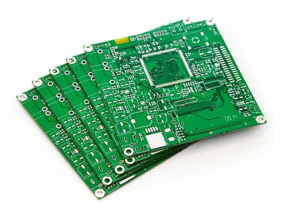
A printed circuit board (PCB) is a substrate that mechanically supports electronic components and electrically connects them through patterned conductive structures, typically copper.
A PCB may contain:
- Copper traces
- Pads
- Vias
- Copper planes
- Solder mask
- Silkscreen
- Through-holes
- Mounting holes
- Component footprints
- Board-to-board or cable connectors
Electronic components are attached to these structures using technologies such as surface-mount technology (SMT) and through-hole technology (THT).
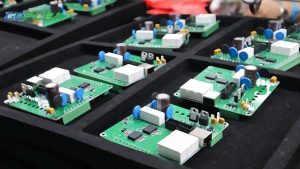
The PCB itself is not necessarily a complete electronic system. A bare PCB provides the physical and electrical infrastructure, while a PCBA contains the components that enable the intended circuit functions.
Types of PCB Components
Understanding the components installed on a PCB board is one of the first steps in learning how to read it.
Electronic components are commonly divided into two broad categories: passive components and active components.
1. Passive Components
Passive components generally do not provide power gain. Instead, they store, dissipate, or control electrical energy and signals.
Resistors
A resistor limits current and creates a specified voltage drop within a circuit. Its resistance is measured in ohms (Ω).
Common resistor types include:
- Fixed resistors
- Variable resistors
- Potentiometers
- Thermistors
- Current-sense resistors
On a PCB, resistors are commonly identified with the reference designator R, such as R1, R2, or R15.
For surface-mount resistors, a numerical code may be printed on the component, although many small packages have no visible marking.
Capacitors
A capacitor stores electrical energy in an electric field and is widely used for:
- Power supply decoupling
- Filtering
- Energy storage
- Coupling and DC blocking
- Timing circuits
- Noise suppression
Capacitors are commonly identified with the reference designator C.
Their capacitance is measured in farads (F), with common values expressed in microfarads (µF), nanofarads (nF), and picofarads (pF).
Different capacitor types have different characteristics. For example, electrolytic capacitors can provide relatively high capacitance, while ceramic capacitors are widely used for high-frequency decoupling.
Polarity must also be considered for polarized capacitors.
Inductors
An inductor stores energy in a magnetic field and opposes changes in current.
Inductors are commonly used in:
- DC/DC converters
- Filters
- Power supplies
- RF circuits
- EMI suppression
The reference designator L is commonly used for inductors, and inductance is measured in henries (H), typically µH or nH in many PCB applications.
2. Active Components
Active components can control electrical signals and, depending on the device and circuit configuration, provide switching, amplification, regulation, processing, or other active functions.
Diodes
A diode is a semiconductor device that primarily allows current to flow preferentially in one direction.
Diodes are used in:
- Rectification
- Reverse-polarity protection
- Voltage regulation
- Signal processing
- Switching
- LED illumination
- Transient protection
They are commonly identified by the reference designator D.
When reading a PCB, pay attention to the diode’s polarity marking and package orientation.
Transistors
Transistors are fundamental semiconductor devices used for switching, amplification, power control, and signal processing.
Common transistor families include:
- BJT
- MOSFET
- JFET
- Other field-effect transistor structures
A transistor package may have three or more terminals depending on its architecture and application. For a conventional BJT, the terminals are collector, base, and emitter. A MOSFET typically has gate, drain, and source terminals.
Transistors are often identified as Q on PCB silkscreen, although reference-designator conventions can vary.
Integrated circuits may contain millions or billions of transistors, depending on the technology and device generation.
Tools for Reading a PCB
Having the right tools makes PCB reading considerably easier.
Technical Documentation
Before examining an unfamiliar board, collect as much documentation as possible:
- Schematic
- PCB layout
- BOM
- Component datasheets
- Assembly drawing
- Fabrication drawing
- Test specifications
- Service documentation
- Gerber files
- Drill files
The more complete the documentation, the less guesswork is required.
Magnifying Glass or Microscope
A magnifying glass or microscope is useful for examining:
- Small SMD components
- Fine-pitch ICs
- Solder joints
- PCB traces
- Pads
- Via structures
- Component markings
- PCB damage
For modern HDI and high-density boards, optical magnification may be necessary to distinguish very small components and routing features.
Digital Multimeter
A digital multimeter (DMM) is one of the most useful instruments for PCB troubleshooting.
Depending on the instrument, it can measure:
- DC/AC voltage
- Resistance
- Continuity
- Current
- Diode characteristics
Continuity testing can help determine whether two points are electrically connected. However, a continuity beep does not automatically mean that a short circuit exists. Parallel circuit paths, low-resistance components, coils, semiconductor junctions, and capacitors can affect measurements.
LCR Meter
An LCR meter can help identify or measure:
- Inductance
- Capacitance
- Resistance
It can be particularly useful when analyzing unknown passive components.
Oscilloscope
An oscilloscope allows engineers to observe actual electrical waveforms.
It can be used to analyze:
- Clock signals
- Data signals
- PWM
- Analog waveforms
- Power-rail ripple
- Transient behavior
For dynamic circuits, an oscilloscope provides information that resistance or continuity measurements cannot provide.
How to Read a PCB Board Step by Step
A structured workflow makes how to read a PCB board much easier to understand.
The recommended approach is to move from the overall physical structure to individual components, then to electrical connectivity and functional blocks.
1. Perform a Visual Inspection
Start with the physical PCB before applying power.
Examine:
- Board shape
- Board dimensions
- Layer appearance
- Component placement
- Connector locations
- Silkscreen markings
- Burn marks
- Cracked components
- Corrosion
- Lifted pads
- Damaged traces
- Missing components
- Broken connectors
The board’s physical characteristics may provide immediate clues about its construction and function.
For example, you may be able to distinguish a simple single-sided board from a double-sided or multilayer PCB based on visible copper features and documentation. However, the exact internal layer count generally cannot be determined reliably from external appearance alone.
2. Identify Power and Ground References
Power is usually the best place to begin understanding an unfamiliar circuit.
Look for:
- DC input connectors
- Battery terminals
- USB or other power interfaces
- Fuses
- Protection components
- Voltage regulators
- DC/DC converters
- Large capacitors
- Power MOSFETs
- Ground connections
Follow the power path from the input toward the major circuit blocks.
A typical power architecture might look like:
Power Input → Protection → Filtering → Regulation → Distribution → Functional Circuits
Ground should be analyzed separately.
Ground may be implemented through:
- Ground planes
- Copper pours
- Ground traces
- Ground vias
- Connector ground pins
On multilayer boards, a ground plane may be hidden inside the PCB, so it may not be visible from the surface.
Do not assume that every large copper region is ground. Use the schematic, net information, test points, and electrical measurements to confirm its function.
3. Identify the Components
Once power and ground are understood, identify the major components.
Look for:
- Reference designators
- Component markings
- Package types
- Polarity indicators
- Pin-1 indicators
- Component orientation
- Manufacturer markings
Identifying Through-Hole Components
Through-hole components are generally easier to recognize because their physical structures are larger.
Examples include:
- Connectors
- Transformers
- Relays
- Large capacitors
- Switches
- Power devices
Identifying SMD Components
SMD components can be much more difficult to identify.
A small package may not provide enough information to determine its exact part number.
When necessary, use:
- Component top markings
- Package dimensions
- PCB reference designator
- Datasheets
- BOM
- Circuit location
- Pin configuration
- Electrical measurements
Never assume that two visually identical SMD components have the same electrical specifications.
4. Read PCB Markings and Symbols
PCB silkscreen and component markings provide valuable information.
Common PCB markings include:
- Reference designators
- Polarity indicators
- Pin-1 markers
- Connector labels
- Test-point labels
- Voltage labels
- Revision numbers
- Product identifiers
- Warning symbols
You may also encounter labels related to:
- ESD precautions
- High voltage
- Battery polarity
- RoHS or other compliance information
- Manufacturing revisions
However, markings can vary between manufacturers and products. They should be interpreted together with the schematic, BOM, datasheets, and other documentation whenever available.
5. Trace the Signal Paths
After identifying components, begin following the copper connections.
A basic signal path may look like:
Input → Protection → Filter → Amplifier/Controller → Processing → Output
Trace connections between component pins and determine where each net goes.
For a multilayer PCB, a trace may disappear into a via and continue on another copper layer.
Therefore, visible surface routing alone may not reveal the complete connection.
Use Net Information When Available
If the native PCB design file is available, use the EDA software’s net highlighting function to follow an entire electrical network.
This is much more reliable than manually guessing connections from a PCB image.
When working only with a physical board, electrical measurements can supplement visual inspection.
6. Understand Test Points, Jumpers, and Switches
Test points are specifically provided locations for probing electrical signals.
They may be labeled:
- TP1
- TP2
- TEST
- GND
- VCC
- Specific signal names
Test points can be useful for measuring:
- Supply voltage
- Clock signals
- Communication signals
- Analog signals
- Control signals
Jumpers and configuration switches may also determine how a circuit operates.
They can be used to:
- Select operating modes
- Configure voltage levels
- Enable or disable functions
- Select communication settings
- Configure hardware options
Always check the product documentation when available because jumper functions and switch settings are application-specific.
7. Analyze Functional Blocks
Complex PCBs are easier to understand when divided into functional blocks.
For example, a typical embedded control board may contain:
- Power supply
- Microcontroller
- Memory
- Communication interface
- Sensor interface
- User interface
- Motor driver
- Protection circuit
Instead of trying to understand every component simultaneously, identify the major blocks first.
Then analyze how those blocks interact.
For example:
Power Supply → Microcontroller → Communication Interface
and
Sensor → Signal Conditioning → ADC → Microcontroller
This block-level approach is especially useful for PCB troubleshooting and reverse engineering.
8. Compare the Physical PCB With the Schematic
If the schematic is available, use it as the logical reference.
The schematic tells you:
- What components are connected
- Which nets are related
- Circuit functions
- Component values
- Power relationships
The PCB layout tells you:
- Where components are physically located
- How traces are routed
- Where vias are placed
- Which layers are used
- How the board is physically constructed
The two should be used together.
A schematic without a layout does not tell you the physical routing, while a layout without a schematic may make circuit functionality difficult to understand.
Reading an Unknown PCB for Reverse Engineering
Reading an unknown PCB is significantly more difficult than reviewing a documented design.
If the original schematic and PCB files are unavailable, reverse engineering may require a combination of:
- High-resolution photography
- Visual inspection
- Component identification
- Datasheet research
- Continuity testing
- Resistance measurements
- Voltage measurements
- Signal analysis
- Layer analysis
- Circuit reconstruction
The board can first be divided into functional regions.
For example:
Power → Processing → Memory → Communication → Input/Output
Each block can then be documented separately.
Important Limitation
A physical PCB does not always reveal internal multilayer connections.
Buried vias, internal copper planes, embedded components, and hidden routing may require advanced inspection techniques or destructive analysis to fully characterize.
Therefore, reverse-engineering results should be verified through electrical testing rather than based solely on visual interpretation.
Practical Tips for Reading a PCB
The following practices can make PCB board reading more accurate and efficient.
Start With Power
Identify the power input and follow the power distribution network before examining complex signal paths.
Identify Major ICs First
Large ICs often define the main functional blocks of a PCB.
Use their markings and datasheets to determine their purpose and pin functions.
Follow Reference Designators
Use R, C, L, D, Q, U, J, TP, and other reference designators to organize your analysis.
Check Pin 1 and Polarity
Component orientation is critical.
Pay particular attention to:
- IC pin 1
- Diode polarity
- Electrolytic capacitor polarity
- LED polarity
- Connector orientation
Use Magnification for Small Components
Many SMD components are too small to identify reliably with the naked eye.
Do Not Assume a Continuity Beep Means a Short
Measure resistance and understand the surrounding circuit before concluding that a short circuit exists.
Review Repairs Carefully
On repaired boards, inspect:
- Jumper wires
- Reworked solder joints
- Replaced components
- Lifted or reconstructed pads
- Trace repairs
- Flux residue
- Damaged solder mask
Previous repair work can provide important clues about the board’s failure history.
Use Documentation Whenever Possible
The original schematic, BOM, layout, and datasheets are significantly more reliable than visual assumptions.
Common Challenges When Reading a PCB
Several factors can make PCB analysis difficult.
Multilayer Routing
Internal copper layers are invisible from the outside, making it difficult to determine complete signal paths from visual inspection alone.
Small SMD Packages
Modern components may be extremely small and may have limited or no visible markings.
Similar-Looking Components
Components with similar packages can have completely different electrical functions.
Damaged Boards
Burned, corroded, or repaired boards may no longer accurately represent their original design.
Missing Documentation
Without the schematic, BOM, or original PCB files, identifying circuit functions can require significant engineering effort.
High-Speed and RF Circuits
High-speed and RF boards require more than simple continuity analysis. Trace geometry, reference planes, impedance, return paths, and component characteristics can strongly affect circuit behavior.
Why Learning How to Read a PCB Board Matters
Understanding how to read a PCB board is useful in many areas of electronics engineering.
PCB Design
Engineers can compare the physical layout with the intended circuit and identify potential design issues.
PCB Troubleshooting
Technicians can locate power rails, signal paths, components, test points, and suspected fault areas.
PCB Assembly Inspection
Assembly engineers can verify component orientation, placement, and soldering against manufacturing documentation.
Product Maintenance
Service personnel can use board information to identify replacement components and diagnose failures.
Reverse Engineering
Engineers can reconstruct circuit relationships when original design documentation is unavailable, subject to applicable intellectual-property and legal requirements.
New Product Development
Studying existing PCB architectures can help engineers understand circuit organization, component selection, thermal management, and layout strategies.
PCB Reading and Manufacturing Support From Kingda
Accurate PCB interpretation is also important before manufacturing and assembly.
For production projects, Kingda can work from the appropriate manufacturing and assembly documentation supplied for the project. Depending on the product, this may include:
- Gerber files
- Drill files
- BOM
- Pick-and-place data
- Assembly drawings
- Fabrication drawings
- PCB specifications
- Stackup information
- Testing requirements
A complete and consistent documentation package helps reduce ambiguity between PCB design, fabrication, and assembly.
For complex projects, customers should ensure that the PCB revision, BOM revision, Gerber package, and assembly data are synchronized before production.
Conclusion
Learning how to read a PCB board requires a combination of electronics knowledge, visual inspection, documentation analysis, and practical measurement skills.
The most effective approach is to start with the physical board, identify the power and ground references, locate major components, interpret reference designators and markings, divide the circuit into functional blocks, and then trace important signal paths.
A schematic explains the logical relationships between components, while a PCB layout explains their physical implementation. Gerber files provide manufacturing artwork, but they should not be confused with the complete editable PCB design database. When these sources are available together, PCB analysis becomes much more accurate.
For an unknown board, tools such as a multimeter, microscope, LCR meter, oscilloscope, datasheets, and component databases can provide additional information. However, multilayer routing, hidden connections, damaged boards, and high-speed circuits may require more advanced inspection and testing methods.
Whether the goal is PCB troubleshooting, design verification, maintenance, assembly inspection, reverse engineering, or new product development, mastering PCB reading can significantly improve the ability to understand how an electronic system works.
With systematic practice, learning to read a PCB can become much like reading an engineering blueprint: start with the overall architecture, identify the major functional blocks, understand the connections, and progressively work down to the individual component and net level.