How to Read a PCB Board: PCB Design & PCB Manufacturing Guide
Printed circuit boards (PCBs) have significantly improved the performance, reliability, and user experience of modern electronic products. By integrating conductive paths and electronic components into a compact structure, PCBs reduce product size, optimize electrical connections, and improve reliability under real-world operating conditions.
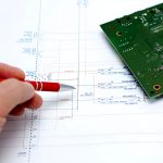
The ability to read and understand a PCB is valuable in many areas of electronics, including engineering education, troubleshooting, product analysis, reverse engineering, repair, and new product development. Engineers may need to interpret a PCB schematic, analyze a PCB Layout, identify unknown components, trace electrical connections, or compare an actual board with its original design.
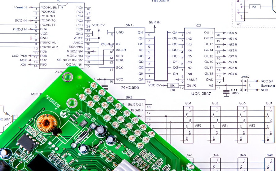
Detailed PCB information is normally documented in technical files and can also be examined directly from a physical board. A PCB schematic provides a symbolic representation of components and their electrical relationships. It is mainly used at the circuit-design level to understand the functional concept of a product.
A PCB layout provides a much more detailed representation of the physical implementation. Layer arrangement, component footprints, placement and orientation, layer-by-layer routing, vias, and the final physical board structure all contribute to understanding how to read a PCB board.
Both schematics and PCB layouts are valuable when analyzing a physical PCB sample. This guide explains the fundamentals of PCB components, the tools used for PCB reading, and a systematic method for analyzing an unfamiliar circuit board.
What Is a PCB?
A printed circuit board (PCB) is a substrate that mechanically supports electronic components and electrically connects them through conductive copper features.
A typical PCB may contain:
- Copper traces
- Pads
- Vias
- Component footprints
- Solder mask
- Silkscreen
- Ground planes
- Power planes
- Through-holes
- Mechanical features
Electronic components are mounted onto the board and connected through conductive paths to form functional circuits. Depending on the application, a PCB can be single-sided, double-sided, or multilayer.
Because PCBs provide both mechanical support and electrical interconnection, they are often considered the backbone of modern electronic products.
Types of PCB Components
Understanding the components used on a PCB and their functions is essential for learning how to read a PCB board.
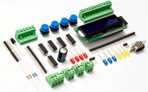
Electronic components are commonly divided into two broad categories: passive components and active components. This classification is based on their electrical behavior and role in a circuit.
1. Passive Components
Passive components generally do not provide signal gain. Instead, they store energy, dissipate energy, or influence electrical signals through characteristics such as resistance, capacitance, and inductance.
Resistors
A resistor limits or controls current and produces a voltage drop according to Ohm’s law. Resistance is measured in ohms (Ω).
Resistors are among the most common PCB components. Different types include:
- Fixed resistors
- Variable resistors
- Potentiometers
- Thermistors
- Current-sense resistors
Power ratings can vary depending on the application, such as 0.25 W, 0.5 W, 1 W, or higher.
On PCB layouts and schematics, resistors are commonly identified with the reference designator R, such as R1 or R25.
Capacitors
A capacitor stores electrical energy in an electric field and is commonly used for filtering, decoupling, energy storage, coupling, and timing applications.
Capacitance is measured in farads (F), with commonly encountered values expressed in:
- Millifarads (mF)
- Microfarads (µF)
- Nanofarads (nF)
- Picofarads (pF)
Different capacitor technologies serve different purposes. For example, electrolytic capacitors are commonly used for relatively high capacitance and power-supply filtering, while ceramic capacitors are widely used for high-frequency decoupling.
On a PCB, capacitors are normally identified with the reference designator C, such as C1 or C10.
Inductors
An inductor stores energy in a magnetic field and opposes changes in current.
Inductance is measured in henries (H), although PCB applications commonly use microhenries (µH) or nanohenries (nH).
Inductors are frequently used in:
- DC-DC converters
- Power filters
- EMI filters
- RF circuits
- Matching networks
- Energy-storage circuits
The standard PCB reference designator for an inductor is generally L, such as L1 or L5.
2. Active Components
Active components can control electrical signals and, depending on the device, provide switching, amplification, regulation, computation, or signal processing functions.
Common active components found on PCBs include diodes, transistors, integrated circuits, voltage regulators, and microcontrollers.
Diodes
A diode is a semiconductor device that primarily allows current to flow more easily in one direction than the other.
Diodes are used in many applications, including:
- Rectification
- Reverse-polarity protection
- Voltage regulation
- Signal processing
- Clamping
- Switching
- Light emission
LEDs are a type of diode that emits light when electrically driven.
On schematics and PCB layouts, diodes are commonly identified with the reference designator D, such as D1 or D5.
Transistors
Transistors are fundamental semiconductor devices used for switching and amplification.
Common transistor types include:
- Bipolar junction transistors (BJTs)
- MOSFETs
- JFETs
- Other field-effect transistor structures
A BJT typically has three terminals called the collector, base, and emitter. MOSFETs instead use terminals such as gate, drain, and source.
Modern integrated circuits can contain extremely large numbers of transistors, making them fundamental to processors, memory devices, controllers, and other complex electronics.
On PCB layouts, transistors are commonly identified using Q as the reference designator, although designator conventions can vary between organizations and software libraries.
Tools for Reading and Analyzing a PCB
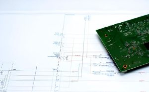
Several tools can make PCB analysis much more effective.
The first resources to consult are technical documents, including:
- Schematic diagrams
- PCB layout files
- Bill of Materials (BOM)
- Component datasheets
- Assembly drawings
- Test specifications
- Manufacturing documentation
- Revision history
For physical inspection, a magnifying glass or microscope can be extremely useful when examining small SMD components, fine-pitch packages, solder joints, and narrow traces.
A multimeter is one of the most useful instruments for PCB troubleshooting and analysis. It can be used to measure:
- Resistance
- Voltage
- Continuity
- Diode characteristics
- Short circuits
- Open circuits
Other instruments may also be required for more advanced analysis.
An LCR meter can help identify capacitance, inductance, and resistance characteristics. Component testers can assist with unknown discrete components, while an oscilloscope can reveal voltage waveforms, timing, noise, and signal integrity characteristics.
The correct tool depends on whether the goal is simple identification, electrical troubleshooting, reverse engineering, or detailed circuit analysis.
Step-by-Step Method for Reading a PCB
A structured PCB-reading process provides a practical way to understand an unfamiliar board.
The process normally starts with visual inspection and documentation review, followed by component identification, power and ground analysis, signal tracing, and electrical verification.
1. Perform a Visual Inspection
The first step in learning how to read a PCB board is careful visual inspection.
Start by examining:
- Board shape
- Board dimensions
- Number of layers, if known
- Component density
- Connector locations
- Mounting holes
- Copper areas
- Silkscreen markings
- Visible traces
- Signs of damage
The physical structure can provide useful clues about whether the board is single-sided, double-sided, or multilayer.
Next, inspect component markings and reference designators. The silkscreen can provide valuable information about component identity, polarity, orientation, connector positions, and test points.
Pay attention to damaged, missing, burned, cracked, or modified components. Incorrectly interpreting a damaged board can lead to incorrect conclusions during troubleshooting or reverse engineering.
2. Identify Power and Ground Reference Points
Power and ground are fundamental to understanding almost every PCB.
Begin by identifying:
- Power connectors
- Battery terminals
- Input terminals
- Output terminals
- Voltage regulators
- Ground points
- Ground planes
- High-current paths
Polarity markings can help distinguish positive and negative connections.
Ground traces or planes may visually resemble other copper structures, so electrical verification may be necessary. A multimeter’s continuity function can help identify connections between suspected ground points.
Understanding the power architecture is especially important because many PCB functional blocks depend on specific supply voltages.
Incorrectly identifying a power or ground connection can lead to incorrect conclusions about the entire circuit.
3. Identify the Components
Components can be identified using a combination of:
- Reference designators
- Package shape
- Component markings
- Pin count
- Pin arrangement
- Polarity
- Physical dimensions
- Datasheets
- PCB footprints
Through-hole (THT) components are often relatively easy to recognize because their leads pass through drilled holes in the PCB.
SMD components can be more difficult to identify because many packages look similar and their markings may be extremely small or abbreviated.
For small SMD components, magnification and a component datasheet or marking database may be necessary.
Integrated circuits require additional attention to package orientation and pin numbering. The location of pin 1 is particularly important when analyzing IC connections.
When the component is customized or its marking is unclear, the BOM, schematic, manufacturer documentation, or PCB manufacturer documentation may provide additional information.
4. Read Additional Markings and Symbols
A PCB often contains more information than the basic component reference designators.
Additional markings may include:
- PCB revision
- Part number
- Manufacturing code
- Date code
- Regulatory markings
- Warning symbols
- ESD warnings
- RoHS-related markings
- Connector labels
- Test-point identifiers
- Voltage information
These markings are often placed near board edges, connectors, mounting areas, or other accessible locations.
Component packages may also contain manufacturer markings, date codes, lot codes, and abbreviated part numbers.
Understanding these markings can help identify the board revision and distinguish between visually similar versions of the same product.
5. Trace the Signal Paths
Once the components have been identified, begin tracing the electrical connections.
A PCB trace may connect one component pin directly to another or may pass through:
- Vias
- Internal copper layers
- Test points
- Connectors
- Resistors
- Capacitors
- Inductors
- Switches
- Protection devices
Visible traces can be followed directly on the outer copper layers. However, internal traces on multilayer PCBs may not be visible from the surface.
In such cases, the native PCB Layout file, schematic, X-ray inspection, electrical testing, or other reverse-engineering methods may be necessary.
When tracing a signal, identify both its starting point and destination. For example, a microcontroller output may pass through a resistor before reaching a connector or another IC.
This systematic approach makes it easier to understand the connectivity of the board.
6. Check Test Points, Jumpers, and Switches
Test points, jumpers, and switches can provide important information during PCB troubleshooting and configuration.
Test points are often labeled with identifiers such as TP1, TP2, or TP3 and provide convenient locations for measuring electrical parameters.
Jumpers may be used to:
- Select operating modes
- Configure voltage options
- Enable or disable functions
- Select communication settings
- Change hardware configurations
DIP switches or other switches may perform similar configuration functions.
The correct settings are normally documented in the product’s technical documentation and may sometimes be printed directly on the PCB silkscreen.
Understanding these configuration elements is particularly useful when diagnosing a board that appears to function differently from the expected configuration.
Reading an Unknown PCB Through Reverse Engineering
Reading a documented PCB is relatively straightforward because the schematic, layout, BOM, and datasheets provide supporting information.
Analyzing a completely unknown PCB is much more challenging.
In reverse-engineering situations, it is useful to divide the board into functional blocks rather than attempting to understand the entire circuit simultaneously.
For example, a board may be divided into:
- Power supply section
- Processing or control section
- Memory section
- Communication section
- Sensor section
- Output or driver section
- Protection section
Each functional block can then be analyzed separately.
The results should be cross-checked through continuity measurements, component identification, voltage measurements, signal measurements, and functional testing.
For complex boards, a reverse-engineered circuit should not be considered reliable until the reconstructed connections and functions have been sufficiently verified.
Practical Tips for Reading a PCB
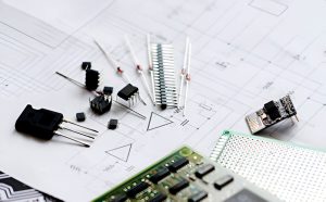
- Check for damaged or modified components. Burn marks, cracked packages, lifted pads, corrosion, and previous repair work can change the original appearance of a board.
- Use magnification for small SMD components. Many SMD packages look almost identical, and their markings can be difficult to read without magnification.
- Understand PCB reference designators. Common designators such as R, C, L, D, Q, U, J, and TP provide useful clues about component types and functions.
- Check component orientation. Pin-1 indicators, polarity marks, notches, dots, and chamfers can help determine the correct orientation.
- Understand SMD marking conventions. Component markings do not always directly represent the full part number. Datasheets and manufacturer information may be required for accurate identification.
- Compare the physical board with the schematic and layout whenever possible. This can reveal component substitutions, design revisions, manufacturing differences, and repair modifications.
- Document every confirmed connection. When reverse engineering, recording verified nets and component relationships reduces the risk of repeatedly analyzing the same area.
- Verify assumptions electrically. A visual interpretation should be confirmed with continuity, resistance, voltage, waveform, or other appropriate measurements whenever possible.
PCB Schematic vs. PCB Layout vs. Physical Board
Understanding the relationship between these three representations is essential for anyone learning how to read a PCB.
| Item | Main Purpose | Information Provided |
|---|---|---|
| PCB Schematic | Electrical design | Components, symbols, logical connections, circuit functions |
| PCB Layout | Physical implementation | Component placement, footprints, routing, layers, vias, board outline |
| Physical PCB | Actual product | Real components, solder joints, markings, materials, modifications, manufacturing condition |
The schematic explains what the circuit is supposed to do.
The PCB layout explains how the circuit is physically implemented.
The physical PCB shows what was actually manufactured and assembled.
Comparing all three can provide a much more complete understanding of a product.
Conclusion
Learning how to read a PCB board is a practical engineering skill that combines electronics knowledge, visual inspection, documentation analysis, and hands-on measurement.
The process begins with understanding the PCB’s physical structure and identifying passive and active components. It then progresses to recognizing power and ground networks, interpreting markings and symbols, tracing signal paths, and examining test points, jumpers, and configuration switches.
For documented products, schematics, PCB Layout files, BOMs, datasheets, and manufacturing documents provide valuable references. For unknown products, reverse engineering requires a more systematic approach based on functional blocks, electrical measurements, component identification, and repeated verification.
A strong understanding of PCB reading is valuable for PCB Design, PCB Assembly, troubleshooting, repair, maintenance, and reverse engineering. As PCB technology continues to move toward higher density, smaller packages, multilayer structures, and increasingly complex circuits, the ability to interpret both digital design files and physical boards will remain an important engineering capability.