How to Repair a Keyboard PCB: PCB Design & PCB Manufacturing Guide
The evolution of electronics has played a major role in the development of modern products and applications. From early computing systems to today’s compact consumer electronics, every generation of computers has relied on advances in electronic engineering and PCB Design and manufacturing technology.
A computer system is supported by multiple interconnected circuit boards, while many peripheral devices contain their own dedicated PCBs. A keyboard is one of the most common computer input devices, and its internal electronics are built around a Keyboard PCB that manages the key matrix, communication interface, indicator LEDs, and other functions.
Although a keyboard PCB is normally protected inside the keyboard housing, it can still experience electrical, mechanical, or environmental failures. Damaged traces, cracked solder joints, corroded contacts, failed components, liquid contamination, and connector problems can all cause keys or other keyboard functions to stop working.
Fortunately, many common keyboard PCB problems can be diagnosed and repaired without replacing the entire keyboard. This guide explains how to diagnose and repair a Keyboard PCB, including trace repair, solder rework, cleaning, component replacement, and final testing.
What Is the Difference Between PCB Repair and Replacement?
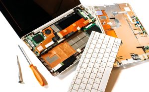
Before repairing a keyboard PCB, it is important to determine whether repair is actually practical.
PCB Repair is generally appropriate when the damage is localized and the board’s main structure remains intact. For example, a broken trace, loose solder joint, corroded contact, or damaged connector may be repairable with relatively simple rework.
Replacement may be more appropriate when the PCB has extensive burn damage, severe corrosion, multiple failed components, damaged internal layers, or other defects that could compromise long-term reliability.
The decision should consider:
- Extent and location of the damage
- Availability of replacement components
- Repair time and labor
- Required reliability
- Availability and cost of a replacement keyboard
- Risk of causing additional damage during rework
For a simple broken trace, repair may be practical. For a severely damaged multilayer board, replacement may be more economical and reliable.
Standard Diagnostic Procedure Before Repairing a Keyboard PCB
A systematic diagnostic procedure is essential before performing any repair. Correctly identifying the failure helps prevent unnecessary soldering, component replacement, or trace modification.
The basic process should include problem identification, visual inspection, electrical testing, component inspection, and firmware or configuration verification where applicable.
Clearly Identify the Problem
Begin by documenting the exact symptoms.
For example, determine:
- Which keys are not responding?
- Are only individual keys affected, or is an entire row or column unavailable?
- Are indicator LEDs working?
- Is the keyboard recognized by the computer?
- Is the USB or wireless connection stable?
- Are there visible broken traces?
- Are any solder pads lifted or damaged?
- Are components missing, cracked, or burned?
- Is there evidence of liquid damage or corrosion?
- Does the problem occur intermittently?
Understanding the symptom pattern can provide important clues about the location of the fault.
For example, if several keys in the same matrix row or column stop working simultaneously, the problem may be associated with a shared PCB trace, switch connection, diode, or controller circuit rather than several independent switches failing at the same time.
Perform a Visual Inspection
A detailed visual inspection should be performed before electrical testing.
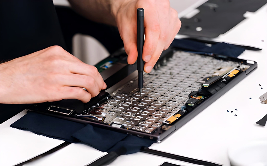
Use adequate lighting and, when necessary, a magnifying glass or microscope to inspect the Keyboard PCB for:
- Burn marks
- Cracked solder joints
- Broken or scratched traces
- Lifted solder pads
- Corrosion
- Liquid residue
- Contamination
- Damaged connectors
- Missing components
- Cracked components
- Mechanical damage
- Damaged switch contacts
Modern keyboard PCBs can contain very small surface-mount components, making magnification particularly useful.
Visual inspection is often the fastest way to identify obvious mechanical or manufacturing-related problems.
Check Connectivity and Continuity
If no obvious physical damage is found, use a multimeter to perform continuity tests.
Before testing, disconnect the keyboard from its power source. Then identify the relevant traces, connector pins, switch contacts, or matrix lines and check whether electrical continuity exists between the expected points.
An open circuit where continuity should exist may indicate:
- A broken PCB trace
- A cracked solder joint
- A damaged via
- A lifted pad
- A failed connector
- A damaged component
Continuity testing is particularly useful for tracing a keyboard matrix problem from the switch area toward the controller.
However, continuity alone does not prove that the circuit is functioning correctly. Some faults involve resistance changes, leakage, short circuits, or component failures that require additional measurements.
Inspect Keys, Switches, and Components
A keyboard PCB typically contains a matrix of switches or switch contacts along with other electronic components.
Depending on the keyboard design, these may include:
- Mechanical or membrane switch contacts
- Diodes
- Resistors
- Capacitors
- LEDs
- USB interface components
- Wireless communication components
- Microcontrollers
- Connectors
- Protection components
If only one key is affected, inspect the corresponding switch, solder joints, and PCB traces first.
If multiple keys are affected, investigate the shared matrix row or column and the associated components.
For mechanical keyboards, a defective switch can sometimes be mistaken for a PCB failure. Therefore, the switch itself should be tested before modifying the PCB.
Check Firmware and Configuration
Some modern keyboards contain programmable controllers and firmware that can affect keyboard functionality.
If the hardware appears to be intact, check whether:
- The keyboard is recognized by the operating system.
- The correct keyboard layout or configuration is selected.
- The firmware version is appropriate.
- The keyboard has recently been flashed or reconfigured.
- A programmable keymap contains incorrect assignments.
- The manufacturer provides a firmware recovery procedure.
Firmware problems should not automatically be treated as PCB hardware failures. If the electrical circuitry works correctly but the keyboard behaves incorrectly, configuration or firmware may be the actual cause.
Common Methods for Repairing a Keyboard PCB
Once the fault has been identified, select the smallest and safest repair method that can restore the original electrical function.
Remove Corrosion and Contamination
Liquid spills, dust, oils, chemicals, and other contaminants can interfere with PCB operation.
Before performing electrical repairs, carefully clean the affected area using an appropriate PCB-safe cleaning method. Isopropyl alcohol is commonly used for removing many types of residue, provided it is compatible with the board and components.
For liquid-damaged keyboards, cleaning should include both the visible PCB surface and areas around connectors, switches, and components where residue may remain.
After cleaning, allow the board to dry completely before reconnecting power.
Cleaning is especially important because corrosion can continue to damage copper traces and component connections even after the original contamination has been removed.
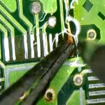
Repair Broken PCB Traces
Broken traces are among the most common localized PCB failures.
For a small break, the damaged copper can sometimes be exposed and bridged using a fine insulated jumper wire. The repair wire should be securely soldered to sound copper on both sides of the damaged section.
The general process is:
- Identify the exact location of the broken trace.
- Confirm the break with a multimeter.
- Carefully remove solder mask from suitable sections of intact copper.
- Apply a small amount of flux.
- Solder a properly sized jumper wire across the damaged section.
- Secure the repair so that it does not move or create a short circuit.
- Check continuity again after the repair.
Conductive ink may be suitable for some very small or low-current trace repairs, but it is not always mechanically robust enough for areas exposed to repeated stress.
For larger or more severely damaged traces, copper foil or copper tape can sometimes be used to recreate the conductor. The repaired section must be mechanically secure and electrically continuous.
When repairing a keyboard matrix, pay particular attention to trace routing and nearby conductors because closely spaced traces can easily create accidental shorts.
Re-Solder Damaged Components
Cracked, cold, or mechanically damaged solder joints can interrupt electrical connections even when the component itself is functioning correctly.
If a solder joint is visibly cracked or detached, remove contaminated or excess solder as necessary, apply an appropriate amount of flux, and reflow the connection using a temperature-controlled soldering iron.
When repairing small surface-mount components:
- Use the correct soldering temperature.
- Apply only a small amount of solder.
- Avoid excessive heating.
- Prevent solder bridges between adjacent pads.
- Use magnification when necessary.
- Avoid applying mechanical force to fragile components.
If a component itself has failed, replace it with a compatible part that matches the original electrical and mechanical specifications.
Repair or Replace Damaged Pads
A lifted or damaged solder pad requires additional care.
If the pad is only partially damaged but the underlying connection remains intact, it may be possible to restore the solder joint.
If the pad has completely separated from the PCB, the repair may require exposing the connected copper trace and creating a mechanically secure alternative connection.
For more serious damage, particularly around connectors, switches, or multilayer structures, a simple solder bridge may not provide sufficient mechanical reliability.
This is one reason why PCB Manufacturing quality and appropriate material selection are important for long-term reliability.
Repair Damaged Connectors
Keyboard connectors can fail because of mechanical stress, repeated insertion and removal, cracked solder joints, or damaged contacts.
If the connector itself is intact but its solder joints are cracked, re-soldering may restore the connection.
If the connector is physically damaged, it should normally be replaced with a compatible component.
After replacement, verify both electrical continuity and mechanical stability. A connector that works electrically but moves excessively may fail again during normal keyboard use.
Reassembly and Functional Testing
After completing the repair, inspect the entire PCB before reconnecting it to the keyboard.
Check for:
- Unintended solder bridges
- Loose wires
- Exposed conductors
- Incorrectly installed components
- Remaining contamination
- Damaged connectors
- Short circuits
- Incomplete solder joints
Reconnect the keyboard and perform a complete functional test.
Test individual keys as well as the keyboard matrix as a whole. If the keyboard includes backlighting, indicator LEDs, macro functions, USB communication, or wireless connectivity, verify those functions as well.
For programmable keyboards, firmware or keymap configuration may need to be restored after hardware repair.
A repaired board should be tested under realistic operating conditions rather than assuming that one successful key press confirms the repair.
Best Practices and Preventive Measures
Following good repair practices can significantly reduce the risk of additional PCB damage.
- Disconnect power before repairing the PCB.
- Use appropriate ESD protection when handling sensitive electronic components.
- Use a temperature-controlled soldering iron for rework.
- Avoid excessive heat, especially around connectors, plastic components, and small surface-mount devices.
- Use compatible replacement components with appropriate electrical ratings.
- Use magnification when working on fine-pitch components or narrow traces.
- Avoid unnecessary scraping of the PCB surface.
- Keep repaired jumper wires properly insulated and mechanically secured.
- Do not allow solder bridges to form between adjacent traces or pads.
- Clean flux and contamination after repair when appropriate.
- Perform continuity and short-circuit checks before applying power.
- Test the entire keyboard rather than only the originally defective key.
- Handle mechanical keyboard components carefully during disassembly and reassembly.
Preventive maintenance is also valuable. Keeping the keyboard away from liquids, excessive humidity, dust, and mechanical impact can reduce the risk of future PCB failures.
When Should You Repair or Replace a Keyboard PCB?
The choice between repair and replacement depends primarily on the extent of the damage.
| Situation | Recommended Approach |
|---|---|
| Single broken trace | Trace repair |
| Cracked solder joint | Re-soldering |
| Minor contamination | Cleaning and inspection |
| Damaged individual component | Component replacement |
| Damaged connector | Re-solder or replace connector |
| Lifted solder pad | Pad repair or trace reconstruction |
| Extensive corrosion | Detailed inspection; replacement may be preferable |
| Burned PCB area | Evaluate structural and electrical damage |
| Multiple damaged circuits | Replacement may be more practical |
| Severe multilayer/internal damage | Replacement is often more practical |
For a simple localized failure, PCB Repair can restore the keyboard at relatively low cost. However, if the board has extensive damage or the repair would require significant rework, replacing the keyboard or PCB assembly may provide a more predictable result.
How PCB Design and PCB Manufacturing Affect Keyboard Reliability
Keyboard reliability begins long before repair.
During PCB Design, engineers must consider trace width, copper thickness, component placement, switch footprints, connector strength, electrical clearances, ESD protection, and mechanical constraints.
During PCB Manufacturing, process control affects solderability, dimensional accuracy, copper integrity, hole quality, solder mask coverage, and overall board reliability.
For keyboards with dense switch matrices and compact layouts, good design practices are particularly important because traces may be closely spaced and difficult to repair.
A reliable keyboard PCB should therefore be designed not only for electrical functionality but also for manufacturability, assembly, testing, and long-term mechanical use.
Conclusion
Learning how to repair a Keyboard PCB requires a systematic approach rather than simply replacing components at random. The repair process should begin with symptom identification, visual inspection, continuity testing, component evaluation, and firmware or configuration checks where applicable.
Common problems such as contamination, broken traces, cracked solder joints, damaged pads, and failed components can often be repaired using appropriate PCB rework techniques. However, severe corrosion, extensive burn damage, multilayer internal failures, or widespread component damage may make replacement more practical.
Whether a keyboard PCB is being repaired, redesigned, or manufactured as a new product, proper PCB Design, PCB Manufacturing, inspection, and testing are essential for achieving reliable long-term performance.