PCB Troubleshooting Guide: PCB Design, PCB Manufacturing, Testing & Repair
As electronic devices become smaller, smarter, and more powerful, manufacturers produce enormous numbers of printed circuit boards (PCBs) every day. To meet the requirements of modern electronics, a PCB must provide functionality, reliability, and manufacturability throughout its service life.
Achieving these goals requires a systematic process that includes PCB Design, prototyping, PCB Manufacturing, assembly, inspection, and testing. However, problems can occur at almost any stage. Design errors, manufacturing defects, damaged components, soldering problems, thermal issues, and unexpected operating conditions can all cause PCB failures.
PCB troubleshooting is therefore an essential part of electronics development and maintenance. A structured troubleshooting process helps engineers identify the actual failure mechanism instead of relying on trial and error. This is particularly important for high-density boards with large numbers of pins, fine-pitch components, multilayer structures, and complex signal paths.
This guide explains why PCB troubleshooting is necessary, which tools are commonly used, how to systematically diagnose a faulty PCB, and which mistakes should be avoided during the troubleshooting process.
Why Is PCB Troubleshooting Important?
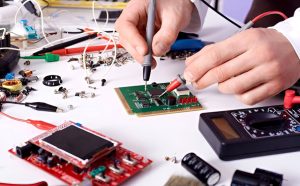
Effective PCB Troubleshooting helps engineers understand what has failed, why it failed, and how the problem can be corrected or prevented. A systematic approach can provide benefits throughout PCB development, manufacturing, and maintenance.
1. Improve Functionality and Reliability
A PCB must be manufactured according to its electrical and mechanical specifications. Defects such as cold solder joints, damaged components, open circuits, short circuits, or incorrect component placement can prevent an electronic system from operating correctly.
By identifying and repairing these problems, engineers can restore the intended functionality of the board and improve system reliability.
For production PCBs, troubleshooting can also help determine whether a failure is isolated or represents a broader manufacturing problem.
2. Improve Production Efficiency
For industrial electronics, PCB failures can result in significant downtime. This is especially problematic when replacement boards are unavailable or the original product has already reached the end of its production cycle.
A structured PCB Testing and troubleshooting procedure allows technicians to quickly evaluate likely failure points and determine whether the board can be repaired, reworked, or replaced.
Instead of replacing an entire board immediately, technicians can often identify and correct a defective component, solder joint, trace, or connection.
3. Improve PCB Design
PCB troubleshooting is not limited to mass production. It is also valuable during prototype development.
When engineers investigate prototype failures, they can identify weaknesses in the original PCB Design, such as:
- Incorrect component selection
- Poor component placement
- Inadequate trace width
- Insufficient power distribution
- Poor grounding
- Signal integrity problems
- Thermal management issues
- Inadequate clearance and creepage
- Manufacturing constraints
The information obtained during troubleshooting can then be incorporated into the next design revision, improving both performance and manufacturability.
4. Reduce Costs
Accurate troubleshooting can significantly reduce unnecessary repair and replacement costs.
For example, if a board failure is caused by a defective capacitor, replacing the entire PCB would waste a functional circuit board. Identifying the faulty component allows technicians to perform targeted PCB Repair or rework instead.
Troubleshooting can be particularly valuable for legacy products whose PCBs are no longer manufactured. Repairing an existing board may be considerably more practical than developing or sourcing a replacement.
What Tools Are Used for PCB Troubleshooting?
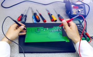
PCB faults should be diagnosed using measured data rather than assumptions. Different failures require different inspection and measurement techniques.
The following tools are commonly used for PCB Troubleshooting.
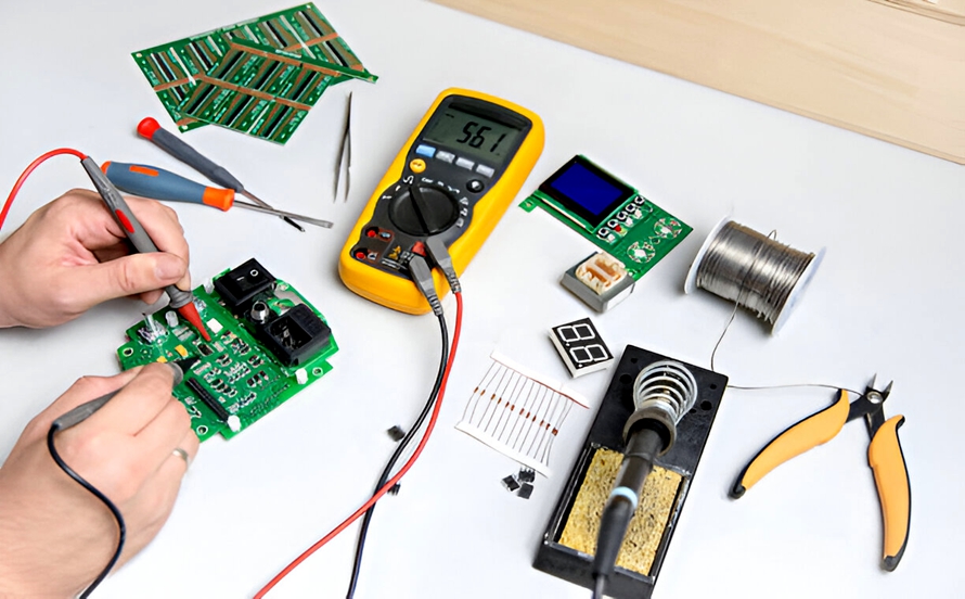
1. Digital Multimeter
A digital multimeter (DMM) is one of the most widely used tools for PCB diagnosis.
It can measure:
- DC and AC voltage
- Resistance
- Current
- Continuity
- Diode characteristics
Resistance and continuity measurements can help identify open circuits and unexpected low-resistance paths. Voltage measurements can also reveal whether power is reaching the correct circuit sections.
However, measurements should always be compared with expected values from the schematic or design documentation rather than interpreted in isolation.
2. Oscilloscope
A multimeter generally provides static or slowly changing measurements, while an oscilloscope allows engineers to observe voltage or other electrical signals as a function of time.
By connecting an oscilloscope probe to an appropriate test point, engineers can observe:
- Clock signals
- PWM signals
- Communication waveforms
- Power-supply ripple
- Transient behavior
- Signal distortion
- Overshoot and ringing
If the measured waveform differs significantly from the expected waveform, this may indicate a power, connectivity, timing, signal-integrity, or component-level problem.
An oscilloscope is particularly useful when a PCB appears to work under static conditions but fails during dynamic operation.
3. Thermal Imaging Camera
A thermal imaging camera provides a non-contact method for observing temperature distribution across a PCB.
Electronic components generate heat according to their power dissipation. Abnormally hot regions may indicate:
- Short circuits
- Overloaded components
- Excessive current
- Failed semiconductors
- Poor thermal management
- Incorrect component operation
Conversely, a component that should normally generate heat but remains unusually cool may not be receiving power or may have an open circuit.
Thermal imaging can therefore help technicians quickly identify suspicious areas without physically touching individual components.
4. Logic Analyzer
A logic analyzer is particularly useful when troubleshooting digital circuits involving microcontrollers, processors, memory devices, and communication interfaces.
It can monitor multiple digital channels simultaneously and display the logical state of signals over time.
Logic analyzers are useful for diagnosing communication problems involving interfaces such as:
- UART
- SPI
- I²C
- GPIO
- CAN
- Other digital control signals
They can help determine whether a device is transmitting the expected data and whether timing or communication errors are occurring.
For intermittent digital failures, a logic analyzer can provide information that may be difficult to obtain with a conventional multimeter.
5. X-Ray Inspection
For multilayer PCBs and complex assemblies, X-ray inspection can reveal defects that are invisible from the surface.
Depending on the equipment and application, X-ray inspection can help identify:
- Hidden solder-joint defects
- Voids
- Internal structural problems
- Certain BGA soldering defects
- Internal PCB abnormalities
This makes X-ray inspection particularly useful for advanced PCB Manufacturing and assembly troubleshooting.
What Are the Steps for PCB Troubleshooting?
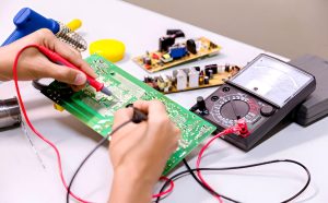
The most effective approach to PCB troubleshooting is systematic rather than based on trial and error.
The following procedure provides a practical framework.
1. Disconnect the PCB From Power
Safety should always be the first priority.
Disconnect the PCB from all external power sources before beginning physical inspection or resistance measurements.
If the board contains capacitors or other energy-storage components, allow sufficient time for discharge or use an appropriate discharge procedure.
Do not assume that a powered-down board is automatically electrically safe.
2. Perform a Visual Inspection
Start with a detailed visual examination of the PCB.
Look for:
- Burn marks
- Discoloration
- Cracked components
- Damaged connectors
- Lifted pads
- Broken traces
- Poor solder joints
- Solder bridges
- Corrosion
- Missing components
- Incorrectly installed components
A microscope may be necessary for fine-pitch components and high-density boards.
Non-destructive inspection methods, such as X-ray inspection, can be considered when the suspected defect is hidden beneath components or within the board structure.
3. Perform Basic Electrical Tests
Use a digital multimeter to verify important electrical conditions.
Depending on the circuit, measurements may include:
- Supply voltage
- Ground continuity
- Resistance to ground
- Continuity between test points
- Diode junction behavior
- Component resistance
Compare measured values with the schematic, datasheet, or known-good board whenever possible.
Unexpected values can provide important clues. For example, an unusually low resistance between a power rail and ground may indicate a short circuit, while an unexpected open circuit may indicate a broken trace, disconnected component, or defective solder joint.
4. Isolate the Faulty Section
Once the general problem area has been identified, divide the circuit into smaller functional sections.
For example, a power-related failure can be investigated by checking:
Input → Protection → Regulation → Distribution → Load
Similarly, a communication problem can be divided into:
Controller → Driver → Transmission Line → Receiver
This approach reduces the search area and makes PCB Troubleshooting more efficient.
5. Test Individual Components
Once a suspected section has been isolated, test the relevant components.
Depending on the component type, technicians may check:
- Resistor resistance
- Diode forward voltage
- Capacitor behavior
- Transistor junctions
- IC supply voltages
- Connector continuity
- Switch operation
When possible, compare measurements with a known-good component or board.
It is important to remember that some components cannot be accurately evaluated using only a multimeter. ICs, capacitors under operating conditions, and high-frequency circuits may require specialized testing methods.
6. Replace or Rework the Faulty Component
After identifying the defective component or connection, follow an appropriate PCB Repair or PCB Rework procedure.
Depending on the failure, the solution may involve:
- Replacing a component
- Resoldering a defective joint
- Repairing a broken trace
- Replacing a connector
- Correcting component polarity
- Repairing a damaged pad
- Reworking an improperly assembled area
After the repair, repeat the appropriate electrical and functional tests.
7. Perform Final Functional Testing
A repaired PCB should not be considered successful simply because the original fault has disappeared.
The board should be tested under appropriate operating conditions to confirm that:
- Power rails are correct
- Signals are functioning correctly
- Components operate normally
- Communication interfaces work properly
- Temperatures remain within acceptable limits
- The original failure does not recur
This final stage helps verify both the repair and the overall reliability of the PCB.
Common PCB Troubleshooting Mistakes to Avoid
Understanding what not to do is just as important as understanding the correct troubleshooting process.
1. Taking Repair Shortcuts
Even when a PCB needs urgent repair, basic non-destructive testing should not be skipped.
Immediately desoldering multiple components without first identifying the suspected failure can create additional damage and make the original problem more difficult to diagnose.
A better approach is to begin with inspection and measurements, then progressively narrow down the fault.
2. Failing to Record Test Results
Troubleshooting can involve many measurements and repeated tests. Without proper documentation, engineers may repeat the same tests or lose important information.
Record:
- Test conditions
- Measurement locations
- Measured values
- Expected values
- Component numbers
- Repair actions
- Final test results
For production environments, this information can also help identify recurring failure patterns.
3. Using Uncalibrated Test Equipment
Accurate measurements depend on reliable instruments.
A multimeter, oscilloscope, thermal camera, or other test equipment that is damaged, improperly configured, or out of calibration may produce misleading results.
Regular calibration and verification should therefore be included in the PCB Testing process.
4. Replacing Components Without Identifying the Root Cause
Replacing a failed component does not necessarily solve the underlying problem.
For example, if a MOSFET repeatedly fails, the real cause could be excessive voltage, insufficient gate drive, thermal stress, incorrect switching timing, or another circuit problem.
Effective troubleshooting should therefore distinguish between the symptom and the root cause.
5. Ignoring the PCB Design and Manufacturing Process
Some recurring failures originate before the board reaches the troubleshooting stage.
A repeated manufacturing defect may be related to soldering, component placement, material selection, drilling, plating, or assembly processes.
Likewise, recurring field failures may indicate an underlying PCB Design issue.
Connecting troubleshooting results with design and manufacturing data can therefore provide much more useful long-term improvements.
How to Improve PCB Troubleshooting Efficiency
A structured troubleshooting system can make diagnosis faster and more repeatable.
Use Schematics and PCB Layout Files
The schematic shows how the circuit is intended to operate, while PCB layout data shows the physical relationships between components, traces, vias, and layers.
Using both documents makes it easier to identify test points and follow signal paths.
Compare With a Known-Good Board
When available, a known-good PCB can be extremely useful.
Engineers can compare:
- Voltage measurements
- Resistance values
- Waveforms
- Component temperatures
- Communication signals
This approach can significantly narrow down the potential failure area.
Establish Standard Test Procedures
For frequently produced PCB assemblies, standardized PCB Testing procedures can improve consistency.
A test procedure may define:
- Visual inspection
- Power-off resistance checks
- Power-rail verification
- Functional testing
- Signal measurement
- Thermal inspection
- Final validation
Standardization makes troubleshooting easier to repeat across multiple boards and technicians.
Conclusion
Effective PCB Troubleshooting is a structured process that progressively narrows down the possible causes of a failure. Instead of relying on trial and error, engineers can combine visual inspection, multimeter measurements, oscilloscope analysis, thermal imaging, logic analysis, X-ray inspection, and other appropriate testing methods to identify the actual problem.
A systematic approach can help determine whether the root cause is a defective component, broken trace, soldering problem, design weakness, manufacturing defect, thermal issue, or signal-integrity problem. It can also reduce unnecessary component replacement and help determine whether a PCB should be repaired, reworked, or redesigned.
For prototype development and mass production, troubleshooting data can provide valuable feedback for improving PCB Design, manufacturing processes, testing procedures, and long-term product reliability. Working with an experienced PCB manufacturer such as Kingda can further support effective diagnosis, manufacturing improvement, and reliable PCB production.