Hydrogen Energy Battery Control Board PCB Design Guide
A hydrogen fuel cell vehicle depends on a control board that watches current, voltage, temperature and pressure at the same time. That board sits between power devices and sensitive sensors, so a small process drift can become a large yield loss. The design and build decisions below explain where those losses start. They also show what an engineer or buyer should verify before the first article is released to production.
The board carries control circuits, power-management devices, communication interfaces and protection logic. It may also link cooling controls and diagnostic paths to the vehicle network. Hydrogen systems can add humidity, thermal stress, vibration and possible corrosive exposure to the usual automotive load. Each of these conditions pushes material choice, copper thickness, plating quality and inspection coverage in a specific direction. Good engineering balances those demands instead of maximizing one of them.
Board Role and Function
A hydrogen energy battery control board is a printed circuit board used inside fuel-cell and power-control systems. It provides the electrical platform that connects sensors, switching devices and processors. Depending on the architecture, it may join voltage and current sensors, temperature sensors, microcontrollers, relays and external vehicle controls. The board must move power and data at the same time without letting one disturb the other. That dual role is what separates it from a simple controller board.
The board is not a passive connection platform. Its copper, dielectric and thermal behavior affect how stable the whole control system stays. A weak thermal path raises component temperature and shortens service life. A narrow high-current trace adds voltage drop and heat. Poor grounding lets switching noise reach low-level measurement signals. Engineers should treat the board as part of the control loop, not as a carrier for parts.
High Current and Thermal Loads
Power-control circuits may carry substantial current, and the exact value depends on the vehicle architecture. Insufficient copper thickness, narrow traces or weak connection structures raise resistance and heat. Designers should size conductors from continuous current, peak current, allowable temperature rise and copper weight. A single copper thickness applied to every design usually wastes cost in one area and creates risk in another. Electrical and thermal analysis should set the copper structure.
Heat removal needs the same care. Power semiconductors, regulators and switching devices create localized hot spots during operation. Large copper areas, thermal vias, copper planes and heat-spreading structures help move that heat away. Metal-core or specialized structures may suit some designs, while external heatsinks and thermal interfaces handle the rest. The board should be judged as part of the full thermal system, together with the enclosure and cooling path.
Via arrays deserve early attention on high-current boards. When a heavy current path changes layers, a single small via becomes a bottleneck and a hot spot. Multiple vias spread the current and lower local heating, but each one must be checked against the drill and plating capability of the fabricator. Designers should confirm via count, drill size and annular ring with the factory before release. A via plan that looks fine on screen can fail at the drill step.
Material and Surface Finish
The laminate should provide thermal stability, electrical insulation, dimensional stability and moisture resistance. It also needs mechanical strength and resistance to thermal cycling. High-Tg materials may be considered when the expected temperature profile calls for better stability. The chosen material must still suit the stackup, the copper structure and the assembly process. A material that performs well alone can fail when paired with the wrong process window.
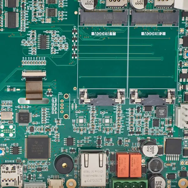
The surface finish forms the solderable interface between copper pads and components. ENIG and other suitable finishes may be considered, depending on package type, assembly technology and operating conditions. Buyers should check surface flatness, solderability, oxidation resistance and pad reliability. Compatibility with fine-pitch parts matters as well. The finish should follow the real assembly and operating requirements, not the lowest quoted cost.
Routing and Signal Integrity
High-current switching paths generate electromagnetic noise that can reach sensitive sensor signals. Designers should plan continuous ground references, controlled return paths and clear separation between noisy and quiet circuits. Differential signaling, local filtering and decoupling capacitors help protect measurement lines. Component placement and connector position also shape the noise profile. A layout that ignores return current will struggle no matter how good the schematic is.
Multilayer construction gives the routing density and electrical separation these boards need. Layers can be assigned to power, ground, high-speed signals and control circuits. The stackup should be fixed before detailed routing, because dielectric thickness and copper weight set controlled impedance. A clear stackup also improves power integrity, EMI behavior and thermal spreading. Skipping this step usually forces a costly redesign later.
A common failure mode is a split ground plane under a sensitive analog trace. The return current detours around the gap and couples noise into the measurement path. The symptom appears as unstable sensor readings that change with load, not as a hard fault. Designers should review plane continuity under every critical signal before release. A short review at layout stage is far cheaper than a board respin after test.
Fabrication Process Control
Lamination control keeps layer registration and dielectric thickness within tolerance. Temperature, pressure, pressing time and resin distribution all affect the result. Poor lamination can cause delamination and dimensional change during thermal cycling. Copper plating must stay consistent on outer layers, inner layers, through-hole walls and vias. Plating uniformity affects resistance and the reliability of interlayer connections, especially on high-current boards.
Drilling accuracy decides whether layers connect as intended. Hole diameter, hole position, drill-to-pad registration and hole-wall quality all need tight control. Aspect ratio limits should be checked against the actual design. A controlled PCB assembly flow starts with fabrication data that matches the engineering release. When copper structures, vias and finishes meet the drawing, assembly and test become far more predictable.
Buyers should ask for the process sheet, not just the certificate. The sheet shows which lamination cycle, plating current and drill program ran on the lot. That record is the quickest way to find the cause when a field return comes back months later. Factories that keep lot data can trace a defect to one machine and one shift. Factories without it can only guess, and guessing usually costs a second lot.

Assembly and Test Coverage
Fabrication is only one stage. Assembly controls decide whether the finished board survives field conditions. Solder-paste deposition, component placement, reflow profile and inspection each feed the next step. High-power parts need sound joints and reliable thermal interfaces, because both affect heat transfer. Accurate SMT PCB assembly with paste inspection, AOI and X-ray where needed catches defects before they reach test.
Test coverage should match the risk. In-circuit test, functional test and burn-in each add confidence, and PCBA testing closes the loop between inspection and process control. When a joint fails, the data should show whether paste, placement or reflow caused it. Buyers should ask for process records, inspection results and test reports. Those records prove that a real control system exists, rather than only on paper.
Voiding under power components is a failure mode worth naming. Large thermal pads can trap gas during reflow, and a voided joint raises thermal resistance. The part then runs hotter than the design assumed, and the board may pass test yet fail in the field. Paste strategy, reflow profile and stencil design all influence void levels. Buyers should agree on an inspection method and a limit before the first lot runs.
Prototype to Production
Hydrogen electronics often need several iterations before release. A typical path runs through schematic review, stackup development, thermal analysis, layout and a design-for-manufacturing check. Prototype builds then reveal excess temperature rise, voltage drop, interference or mechanical conflicts while changes are still cheap. Rapid PCBA prototyping shortens that loop and lets engineers validate component choices early. Once the design is proven, process parameters can be standardized for repeat runs.
Component supply deserves attention during design, not after. Lifecycle status, lead time, approved alternatives and package availability all affect continuity. Counterfeit-risk control and traceability matter on automotive programs. Strong quality management covers incoming material checks, in-process monitoring and final inspection across the whole chain. Buyers who review these records before the first article avoid rework later. The practical takeaway is simple: agree the copper, stackup, finish and test plan in writing before tooling starts.
One last check belongs in every purchase order. State the copper weight, the stackup, the finish and the acceptance limits in the drawing, and require the first article to be measured against them. A clear document removes debate when a lot is questioned. It also gives the fabricator a fixed target for every repeat order. Boards built to a written specification are easier to compare, easier to audit and far easier to keep consistent across batches.