Laser Direct Imaging for Fine Line PCB Fabrication
Imaging is where a circuit pattern is transferred from data into photoresist, and for decades that meant a film and a lamp. Laser direct imaging replaces the film with a scanned beam, removing a whole class of distortion problems and making fine-line production practical. The technology is not simply an upgrade of an old step; it changes how registration, scaling, and yield have to be managed.
What Laser Direct Imaging Changes in the Imaging Step
Conventional imaging places a phototool in contact with the resist and exposes the whole panel at once through a lamp. Laser direct imaging writes the pattern point by point with a modulated beam, using the panel’s own fiducials to place every feature. Because there is no film, there is no film shrinkage, no contact damage, and no wear that gradually degrades the artwork.
The practical consequences reach further than the imaging step. Panels can be scaled individually to compensate for lamination movement, and different products can be imaged in sequence without changing a tool. That flexibility is what allows a shop to run prototypes and production on the same line without the setup cost that film imposes.
How LDI Works: Laser, Optics and Photoresist
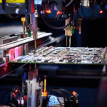
A laser direct imaging system generates a beam, splits and modulates it into many channels, and sweeps it across the panel through a rotating polygon or a similar scanner. The stage moves the panel while the optics write, and the two motions are coordinated so that the pattern lands where the data says it should. Alignment is confirmed by reading fiducials on the copper or on the laminate.
The resist must match the laser wavelength and power. Conventional diazo resists are far too slow, so LDI uses photoresists sensitised to the laser, typically in the near-ultraviolet or violet range. Sensitivity, coating thickness, and the exposure dose all interact, which is why switching to LDI usually means requalifying the resist and the develop line rather than only buying a machine.
Advantages over Contact and Projection Printing
Contact printing presses a film against a resist that may still be tacky, and every particle or surface defect becomes a printable artefact. The film itself stretches, wears, and accumulates defects, and each new artwork requires a new tool with its own lead time and cost. Projection printing avoids contact but loses resolution as the image scale increases.
Laser imaging eliminates the tool, so artwork changes are instantaneous and the defect sources associated with film handling disappear. It also delivers better line-width uniformity across the panel, because the beam dose is controlled electronically rather than depending on lamp uniformity and film contact. The result is tighter distribution of trace widths, which matters more as lines get thinner.
Fine Line Capability and Resist Selection
Fine-line capability depends on the resist as much as the imager. Thinner coatings improve resolution but offer less protection during etching, so the choice is a balance between the smallest feature and the etch resistance required. Positive and negative resists behave differently in this respect, and the develop process must be tuned to match.
Laser spot size, focus, and the number of channels set the addressability of the machine, while the resist sets the contrast. A high-contrast resist produces straighter sidewalls and better tolerance to dose variation. Shops pushing below 50 micrometres generally standardise on a specific resist and imager combination and treat deviations from it as experimental.
Registration and Scaling to the Panel
Laminate moves during lamination and during the bake cycles that follow. With film, that movement has to be absorbed by generous annular rings or by choosing a film that happens to match. With direct imaging, the system measures fiducials and applies a transformation, scaling and rotating the pattern so that it lands correctly on the copper that is already there.
The transformation can be a global fit or a local one, depending on the machine and the number of fiducials read. Local fits handle twist and non-uniform shrinkage better but take longer and can distort the pattern if the fiducials themselves are unreliable. The choice belongs in the process specification, together with the fiducial design and the number required.
Throughput, Cost and Where LDI Fits
Direct imaging is slower per panel than a flood exposure through film, and that gap widens as resist sensitivity falls and the required dose rises. Machines compensate with more laser channels and faster stages, but the capital cost remains high. The economic case rests on eliminating film tooling, reducing touch-up, and improving yield on fine-line products.
High-volume, coarse-line products may still run better on conventional lines, while quick-turn shops, HDI work, and products with frequent revisions benefit most from the flexibility. Evaluate the decision on total cost per good panel rather than on imaging speed alone, since downstream savings often exceed the imaging step’s contribution.
Resist Handling, Coating and Development
Because the resist is exposed directly, its surface condition matters more than it does with film. Coating thickness must be uniform, edges must be clean, and the resist must be dry enough not to mark, yet not so dry that sensitivity drops. Roller coating, curtain coating, and dry film lamination each have their own LDI implications.
Development then determines whether the imaged pattern survives as intended. Over-development opens lines too far and thins the resist shoulders; under-development leaves residue that blocks etching. Because LDI produces sharp latent images, the develop window is often narrower than the resist’s nominal specification suggests, so control of concentration, temperature, and conveyor speed becomes critical.
Process Control and Yield Monitoring
Dose and focus drift slowly, and their effects appear as line-width change rather than as a sudden defect. Measuring a test pattern on every panel, or on a defined sample, gives the data needed to correct the machine before the shift ends. The same measurements feed the etcher, which can adjust to hold the finished width.
Fiducial read failures are the other common signal. A dusty fiducial, a marginal contrast difference, or a poor choice of feature can cause the machine to reject a panel or to align it wrongly. Track the read rate and clean the optics on schedule, because a dirty window reduces beam power and gradually changes the effective dose.
Common Defects and Troubleshooting
Typical LDI problems include open traces from under-exposure, shorts from over-exposure or resist residue, ragged edges from focus error, and misregistration from a bad fiducial fit. Each has a different corrective action, and the first step is to separate machine faults from resist and develop faults by imaging a reference pattern and measuring it.
Keep the resist lot, coating thickness, dose, focus setting, and develop parameters in the lot record. When a defect appears, this data usually identifies whether the imager, the coating line, or the developer changed. Documenting the settings that produce good panels also shortens the learning curve when a new product with finer features is introduced.
Related reading: our fabrication notes, board quality and design release notes cover the same ground.
FAQ
Does LDI remove the need for artwork films entirely? It removes them from the imaging step, though many shops still keep film for legacy processes or as a backup. Digital data replaces the tool, so revisions no longer require a new film, which is the main reason quick-turn and prototype work benefits so much from the technology.
Is LDI suitable for coarse-line boards? It can image them, but the throughput penalty and capital cost make it hard to justify when a conventional line already produces good yields. The value comes from fine features, frequent revisions, and the freedom from tooling, not from printing wide traces better.
What resist should be used with laser imaging? Use a photoresist specified for the laser wavelength and power of the imager, and qualify the coating thickness and develop process alongside it. A conventional film resist will not expose at a practical dose, and mixing resist types on one line makes the process impossible to control.