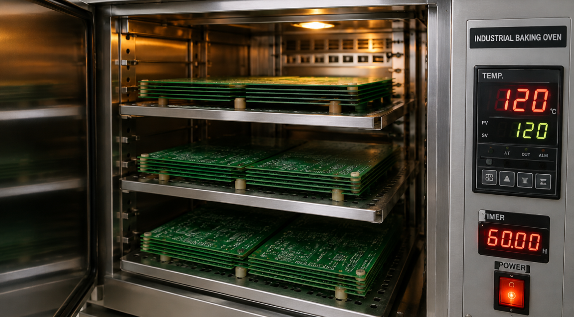
Laser Marking and Traceability on PCB Assemblies
A mark on a board is useful only if it can be read. A laser mark that is applied to the surface has to survive every process step that follows it, and the reading has to work at the stations where it is used rather than only in the marking machine.
What a Board Mark Carries
The mark carries the part number, the revision, the date code, the lot and increasingly a two dimensional code that links to a data record. The code is only worth having if the record it points to exists and is maintained.
Where the mark is used for traceability through assembly, it has to be readable on the assembled board, which means it cannot be placed where a component or a coating will cover it. Our silkscreen notes describe the marking that is printed rather than lasered.
Contrast and How It Is Produced
Contrast comes from one of three sources: removing the solder mask to expose laminate, carbonising the mask, or ablating a coating to reveal a different material underneath. Each produces a different contrast and a different level of damage to the surface.
The choice is usually made from the surface finish. A mark on bare copper reads differently from a mark on mask, and a mark on a plated surface can be destroyed by the plating itself. Our fabrication notes describe where that decision is recorded.
Read Rate and the Reader
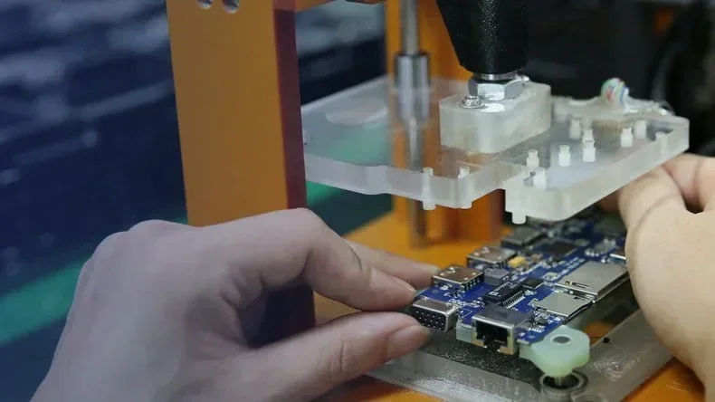
Read rate is a property of the code and the reader together, so a code that reads on the marking machine may fail at the assembly station. The verification has to be done with the reader that will actually be used rather than with a bench reader.
Lighting is the usual reason for the difference. A code with low contrast reads under a diffused ring light and fails under a low angle light, and the two lighting conditions are common at different stations on the same line.

Damage and the Marking Parameter Window
Laser marking removes or changes material, and too much power damages the mask or the laminate underneath. The damage may not be visible at the time and can appear as a lifted mask after reflow or as a conductive path where the mark crossed a conductor.
The parameter window is therefore established between readability and damage rather than at the setting that produces the darkest mark. Where the mark is placed over a plane, the window is narrower because the dielectric is thin.
Placement Rules
Marking is normally kept off conductors, off the solder dam and off areas that will be covered by a component or a coating. It also has to stay clear of the edges that the router will cut and of the areas where a fixture will grip.
Where the board is small and the mark has to be placed in a busy area, the decision is a design compromise rather than a process one, and it is worth making it deliberately. A mark that is unreadable after assembly has no traceability value even though it was applied.
Verification Before Production
Before a production run, the code is verified after the steps that follow it, which is normally after reflow and after any coating. A code that survives marking and fails after reflow has been verified at the wrong point in the flow.
That verification is a first article activity rather than a routine one. It is also the step that catches a mark placed too close to a reflow shadow or to a coating dam. Our first pass yield notes describe how the result is fed back.
Data Handling and the Record Behind the Code
A unique code per board is only useful if the process data is recorded against it. That means the code is read at each station and the result is attached to the record rather than counted at the end of the line.
Doing that turns a traceability mark into a process tool, because the failure of one board can be compared with the data of the boards around it. The cost is the reading and the data handling, and that cost is what decides whether a unique code is worth using.
Process Control and Verification
Keeping a sample from the panel turns a dispute into a measurement, because the same coupon can be re-examined by both parties without rebuilding the batch. Reviewing the design before the data is released is cheaper than correcting it after the panel is in the tank, because every step downstream inherits the decision made at the front end.
Documenting the assumption is part of the design work, and a short note on the drawing prevents a question that would otherwise arrive a day later and cost a day of schedule. The process window is set by the narrowest step in the flow, so an improvement anywhere else shows up as margin rather than as yield until that step is addressed.
FAQ
Can a mark be added after assembly? It can be lasered onto the surface then, and the mask damage risk is lower because there are no further thermal excursions. The placement options are more limited.
Does a darker mark read better? Not necessarily. Readability depends on contrast and geometry, and a darker mark made with more power may damage the surface underneath.
What does gopcb provide for marking and traceability? We provide marking method selected against the finish, parameter windows established between readability and damage, placement rules that keep the code readable after assembly, verification after reflow and coating, and records that tie each code to its process data.