
Multilayer PCB Via Spacing: Hole-to-Hole and Hole-to-Trace Design
Via spacing is one of the quiet decisions that decides whether a multilayer board builds cleanly. Routing density gets the attention, but the gap between two drilled holes and the gap from a hole to nearby copper drive yield. A design that sits at the process limit leaves no room for normal variation. This guide covers the two spacing rules that matter most and how to set them with margin.
Every drilled hole carries a positional tolerance, and every lamination cycle shifts inner layers slightly. Those two effects combine on the finished board, not in the CAD file. A layout that looks compliant on screen can still produce thin annular rings after fabrication. Engineers should treat spacing as a process requirement rather than a drawing formality. The checks below apply to any high-density design, and they pair well with the discipline described under quality management.
Why Via Spacing Drives Yield
When two holes sit too close, the material web between them becomes thin. The drill bit meets uneven mechanical loading as it enters the second hole. Heat dissipation around the bit also changes, because less material surrounds the cut. These effects raise the risk of bit wander, smear, and rough hole walls. Each of those defects can survive electrical test and still weaken the plated connection over time.
The same logic applies to the distance between a via and a trace. A via carries an annular ring on each layer it connects. If that ring sits close to copper on another net, the manufacturer must hold electrical clearance. When the design leaves too little room, CAM engineers reduce or clip the ring. The pad shrinks, the copper support around the barrel drops, and the via becomes less robust. Spacing therefore protects both manufacturability and long-term reliability.
Hole-to-Hole Spacing Rules
Hole-to-hole clearance is measured from the edge of one finished hole to the edge of the next. Center-to-center distance is not the design number, because it hides the drill diameter. Two vias with large finished holes need more center distance to keep the same edge clearance. Designers should convert every rule to edge-to-edge terms before they check the layout. This avoids false confidence when hole sizes differ across the board.
The required edge clearance depends on the drill process, the material, and the panel thickness. Thin webs between holes are harder to drill without breakout or resin damage. Dense via clusters used for thermal relief deserve extra attention, because several holes compete for the same small area. A practical approach is to set a house rule above the supplier minimum and hold it everywhere. Consistency makes the rule easy to audit during review.
Via-in-pad and stacked structures change the picture. When vias share a pad or sit in a tight array, the web between them is thinner than a single isolated hole suggests. Buyers should confirm that the fabricator can drill the array without special tooling or extra cost. Asking early is cheaper than reworking the panel after the first article. The answer also shapes how much copper remains around each barrel.
Hole-to-Trace Clearance
The clearance from a via hole to a trace involves two separate gaps. One is the electrical clearance between the annular ring and the adjacent copper. The other is the fabrication clearance the drill and registration processes need. Designers often check the first and forget the second. A rule that covers only electrical spacing can still fail at the drill step, because the ring has no room to survive tolerance.

Consider a six-layer board where the hole edge sits six mil from a trace edge and the ring is four mil wide. The remaining ring-to-trace gap is only two mil. If the process needs three mil, the CAM engineer must trim the ring to comply. That trim reduces the effective pad and weakens the via. The lesson is simple: budget the ring width and the clearance together, not one at a time.
Inner layers add another constraint. Planes and pours sit close to vias by design, and thermal relief spokes reduce the copper available. A via near a plane edge can lose its ring during clipping, especially when the net spacing is tight. Reviewing these locations on every layer, not just the top, catches problems that a single-layer view hides. Teams planning dense builds can compare options through rapid PCBA prototyping before committing to volume.
Registration and Drill Tolerance
Lamination stacks multiple cores and foils, and each core can shift a little during the press cycle. The result is inner-layer registration that differs slightly from the CAD data. Drilling adds its own positional tolerance on top of that shift. When a via already sits at the minimum clearance, a small deviation in one direction can thin the ring unevenly. In severe cases the hole breaks through the ring entirely.
A board may still pass electrical test after that breakout. Continuity holds, and the net works on the bench. The problem is mechanical, not electrical, so functional test does not flag it. Insufficient copper around the barrel reduces support during thermal cycling and handling. Over a product lifetime, that weakness can turn into an open or an intermittent fault. Spacing margin is the cheapest insurance against this failure mode.
Stackup and Material Effects
Material choice influences how much margin a design needs. Thick panels and high copper weights resist drilling and increase bit wear. Resin systems with different glass styles behave differently under the same drill program. A stackup built from several cores has more registration variables than a simple construction. Designers should match the spacing rule to the actual stackup, not to a generic default.
Copper thickness also matters. Heavy copper plating narrows the gap between features after processing, because the deposit adds material to walls and surfaces. A clearance that looked adequate in the design file can close up on the finished board. Fabricators account for this in their process, but the design must leave room for it. Reviewing the stackup with the supplier before release removes guesswork from the spacing decision.
DFM Checks Before Release
A design rule check catches many spacing errors, but it only enforces the numbers you enter. The rule set should reflect the fabricator’s real capability plus a working margin. Run the check on every layer and confirm that hole-to-hole and hole-to-trace rules both fire. Then review the flagged locations by hand, because dense areas often need judgment rather than a pass or fail. Document any accepted exception with a reason.
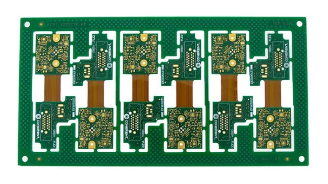
Ask the fabricator for a DFM report before tooling starts. The report should list any clipped annular rings, thin webs, and clearance exceptions. Compare those findings with your own review and resolve disagreements early. A short engineering question at this stage costs a message, while a guess can cost a panel lot. Buyers who want a structured check can pair this with SMT PCB assembly planning so fabrication and assembly reviews share one data set.
Buyer Verification Points
Buyers should confirm the agreed spacing limits in writing before the order is placed. The document should state edge-to-edge hole clearance, ring-to-copper clearance, and the minimum annular ring width. It should also note which stackup and copper weight the numbers assume. Vague statements about standard capability are hard to enforce later. Clear numbers make the first article a real test of the agreement.
At first-article approval, check the actual drilled panels against those limits. Look for clipped rings, off-center holes, and thin webs in the densest regions. Keep the inspection record with the lot so repeat orders can be compared. When a parameter drifts, the record shows whether the change came from the design or the process. Programs that need volume supply should review high-volume PCB assembly early, because spacing rules affect panelization and throughput.
Test coverage closes the loop but does not replace spacing margin. Electrical test confirms continuity, and PCBA testing confirms function under power. Neither measures the copper left around a barrel. That is why the spacing review belongs to the design and fabrication stages, where the geometry is still adjustable. A buyer who asks for the DFM report and the first-article record has the evidence needed to judge supplier consistency.
Practical Design Takeaways
Set hole-to-hole and hole-to-trace rules above the supplier minimum, then hold them across the whole layout. Convert every rule to edge-to-edge terms so drill diameter cannot hide a violation. Budget the annular ring and the electrical clearance as one combined number. Check inner layers as carefully as the outer ones, especially near planes and pours. These habits cost little at design time and prevent expensive rework later.
Finally, treat spacing as a process agreement rather than a drawing detail. The fabricator’s drill tolerance, registration control, and plating process all act on the gap you specify. A design with margin absorbs normal variation and still yields a solid ring. A design at the limit depends on everything going right. For engineers and buyers, the safer choice is to leave room and verify it with records at the first article.