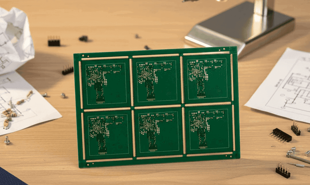
Panel Design for Maximum Material Utilization and Yield
Panel design is where a board’s unit cost is largely decided, long before the first laminate is cut. How many boards fit, how much material is wasted at the edges, how easily the array can be assembled and how cleanly it can be separated all come from decisions made on the panel drawing. This article explains how to reach a panel design that maximises material utilization without creating assembly or depaneling problems.
Why Panel Design Sets Cost
Material is a large share of fabrication cost, and the fraction of each panel that becomes product rather than scrap is the single biggest lever available. A panel that fits four boards where five would fit wastes twenty percent of the laminate before any process is applied.
Utilisation is not the only term, though. A tighter panel may reduce material waste while increasing assembly difficulty, forcing slower placement or adding handling steps that cost more than the material saved. The panel should be evaluated against total cost rather than against material alone.
Border Rails and Tooling Features
Most panels need a border rail along the edges to carry tooling holes, fiducials and the conveyor support area. The rail width is set by the assembly equipment and by the handling requirements, and it is excluded from the usable area when utilisation is calculated.
Tooling holes and fiducials belong in that rail rather than on a board wherever possible, so that they do not consume product area and so that they remain available after a board is removed. Their positions must match the equipment at the assembly house rather than a generic template.

Where the panel will be depaneled before assembly, some of those features must be on every individual board instead, which changes the utilisation arithmetic and should be checked early.
Spacing Between Boards
Boards are separated by a router path or by breakaway tabs, and the gap between them must be wide enough for the cutting tool and for the tolerance of the process. Too narrow a gap causes tool breakage or damage to adjacent boards, while an unnecessarily wide gap wastes material.
Spacing also affects assembly. Boards placed too close together make stencil printing uneven and can interfere with nozzle access during placement, particularly where tall components sit near the panel edge.
Breakaway Tabs and Depaneling
Tabs hold the board in the panel and are removed after assembly, either by hand, by a router or by a punch. Their number, width and position determine how much stress is applied to the board during separation, and stress is the enemy of solder joints and of brittle components near the edge.
Tab placement should avoid sensitive areas, and where a component must sit near a tab, the joint should be reinforced or the tab moved. Perforated tabs reduce the force needed to break them but leave a rougher edge that may need cleaning.
Utilisation Arithmetic and Edge Exclusions
Utilisation is the product area divided by the panel area, and both terms need care. The usable panel area excludes the rails, the tooling zone and any area the conveyor or the printer cannot reach. The product area includes only boards that will actually yield, not the ones lost to edge defects.
A panel that looks efficient on paper often loses a percent or two because boards placed near the outer edge see more process variation and a higher defect rate. Positioning critical boards away from the panel edge is a cheap improvement.
Panel Size Against Equipment Limits
Every machine in the line has a maximum and minimum panel size, and the panel must satisfy all of them rather than the widest one. Printers, placement machines, reflow ovens and cleaning equipment all have limits, and the smallest maximum among them sets the constraint.
Small panels create their own problem. Below a certain size the board cannot be conveyed reliably, so small products are usually assembled in arrays or on a carrier. That decision belongs in the panel design, not in a late conversation with the assembly house.
Array Configurations and Routability
Boards can be arranged in a simple grid, in a mirrored pair or in an interlocked layout that improves material usage. Mirroring can also help assembly where the board has an asymmetric component distribution, since it balances the placement load across the panel.
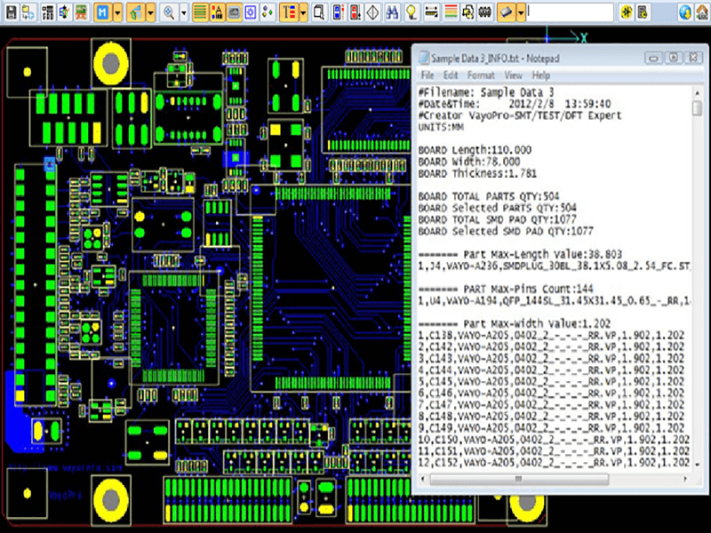
Routability matters as much as area. The router needs a continuous path around every board and enough clearance to turn at corners, and a layout that leaves an enclosed area forces a different depaneling method or a redesign.
Yield Loss and Rework Access
A dense panel raises the value at risk. If one board in a large array fails and the panel must be reworked, the whole panel is exposed to the rework heat. Access for rework should therefore be considered at panel design stage, especially where the product contains large or expensive components.
Where rework is likely, an arrangement that groups boards by function or by component population can limit the impact of a single repair. That is a design decision, and it has to be made before the panel is released.
Documenting the Panel Drawing
The panel drawing should show board positions, rail widths, tooling and fiducial locations, tab positions and widths, the rout path and the direction of the material grain where it matters. It should also state the panel dimensions and the tolerance on each feature.
gopcb reviews panelisation with customers because the drawing is a shared document between fabrication and assembly, and an ambiguity in it costs time in both places. Settling tab placement, rail width and panel size early is one of the cheapest improvements available to a new product, and it protects the quality of every board on the panel.
In practice, material utilization is rarely maximised by geometry alone. The panel that fits the most boards is not always the panel that produces the most good boards, because boards near the rail edge see more variation in etching, plating and printing, and because a dense array is harder to inspect and to repair. Comparing two candidates on cost per good board rather than on area is the test that matters.
A useful habit is to review the panel drawing alongside the assembly drawing before either is released. That conversation takes minutes and surfaces conflicts which would otherwise appear as a tooling delay, such as a rail too narrow for the conveyor, a fiducial hidden under a component or a tab sitting directly beside a brittle package. Resolving them on paper costs nothing.
FAQ
How much material utilisation should I expect? It depends on board size and shape, but well designed panels usually land between seventy and eighty five percent of usable area. Irregular outlines and small boards lose more to rails and spacing.
Can I put tooling holes on the boards instead of the rail? Yes, and it is necessary when boards are depaneled before assembly. Otherwise keep them in the rail so they do not consume product area.
Do breakaway tabs damage components? They can, because separation applies mechanical stress. Keep tabs away from brittle components, support the board during separation and consider routing where the risk is high.