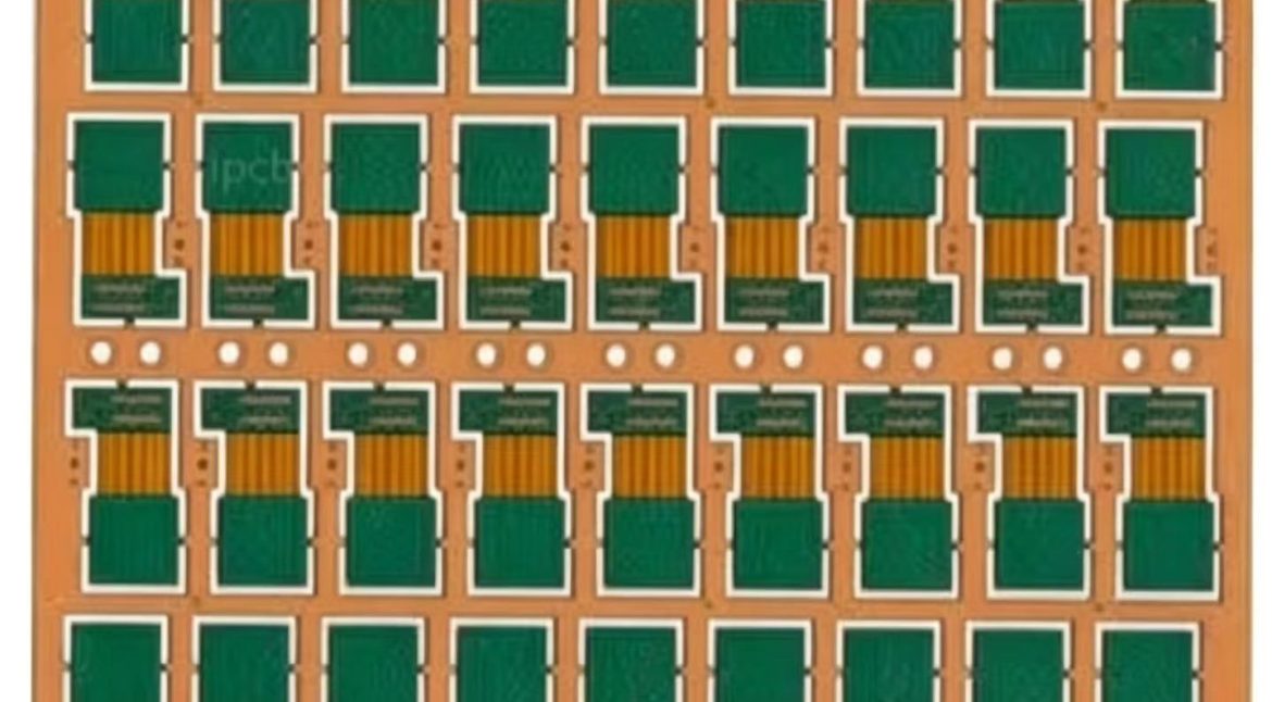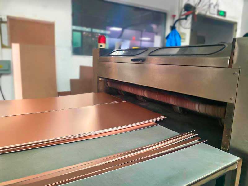
Single-Sided PCB Design and Double-Sided Boards: Structures and Uses Not every product needs eight layers. A large share of electronics, from power supplies and relays to LED drivers and simple instruments, is built on one or two copper layers, and those boards are successful because the design was matched to…
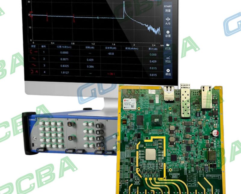
PCB Layout Review: Four Checks Before You Release the Board The review that happens after the routing is finished is the last chance to catch problems before tooling is committed. At that stage the electrical intent is fixed, so the questions shift to whether the board can be built, whether…
PCB Design Workflow: Ten Steps From Schematic to Release Files Board design fails more often from missing inputs than from bad routing. A layout engineer who receives an incomplete schematic, an approximate mechanical drawing, and a verbal description of the stackup will produce a board that matches none of them…
Tapping Test and Drop Test in Electronics Production Between final assembly and electrical test, a manufacturing line usually has one or two mechanical screening stations that look crude compared with the rest of the process. A product is tapped with a rubber ball on a stick, or dropped onto a…
Interference Suppression in Digital Circuit and Microcontroller PCB Design Interference problems are much cheaper to prevent than to cure. A board that is laid out without considering them will usually still work, and then fail intermittently in the field, which is the most expensive kind of failure to diagnose. The…
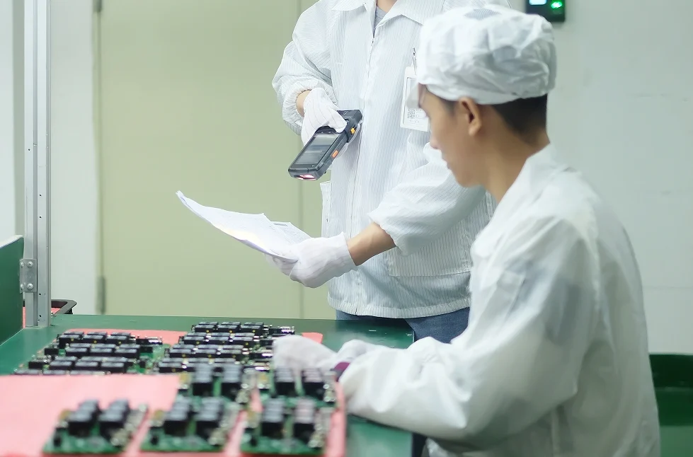
PCB Time Domain Reflectometry Testing: What Matters on the Production Line Buyers and engineers often focus on the finished product and forget the production line behind it. In practice, most field failures can be traced back to process decisions made during assembly. Understanding PCB time domain reflectometry testing gives you…
Multilayer PCB Prototyping: Inner Layer, Lamination and Drilling A prototype build is where a design stops being a schematic and becomes an object that can be measured. The purpose of the first panels is to prove the stackup, the registration and the finish, not only the netlist, and that makes…
PCB Acoustic Microscopy for BGA: From Prototype to Volume Production Electronics manufacturing has become a discipline of small details. Solder paste volumes, placement accuracy, temperature profiles and inspection limits all add up to the final result. This guide looks at PCB acoustic microscopy for BGA from the perspective of a…
Micro Assembly Technology for Small Batch SMT Micro assembly is the practice of placing bare die and very small components onto a high-density interconnect substrate and sealing the result into a single package. It is the technology behind multi-chip modules, sensor packages and the compact radio and power modules that…
PCB Electrical Test: Coverage and the Cost of Missing It Every board that leaves a fabricator is tested for continuity and isolation, and the test is treated as a formality by most designers. It is not. The cost of a defect depends enormously on where it is found, and the…