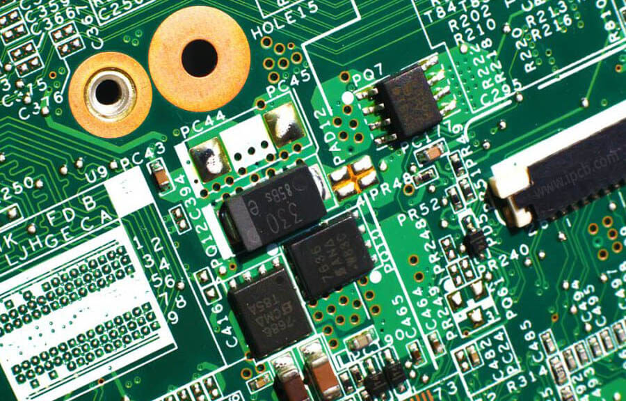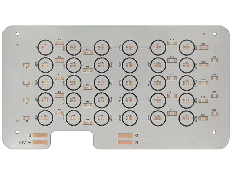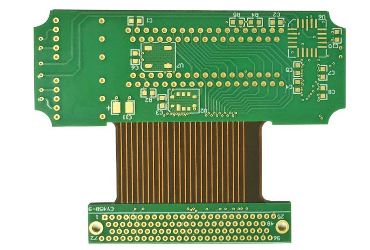
PCB Sampling Plan for Outgoing Inspection: Key Process and Quality Checks Modern electronics depend on boards that are assembled correctly the first time. Every product – a phone, a charger, a medical instrument or an industrial controller – relies on thousands of solder joints that must conduct current for years.…
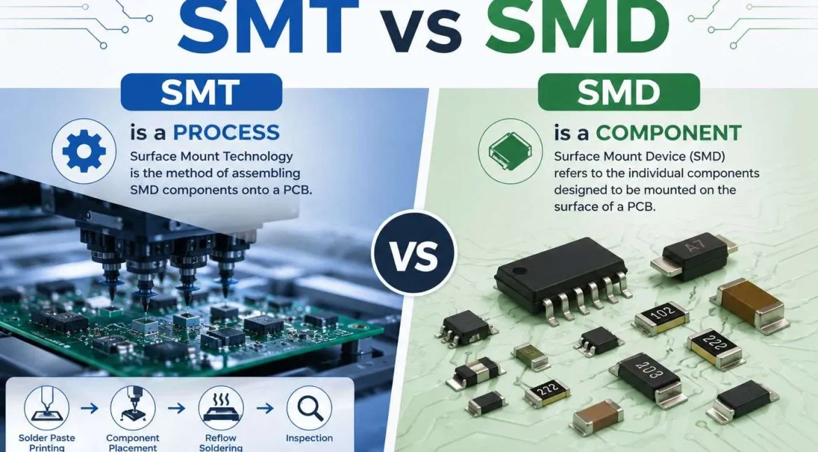
PCB Electrical Test Methods: Flying Probe and Grid A finished board that leaves the shop with an undetected open circuit does not simply get scrapped. It travels to the assembly line, collects components, passes through reflow and possibly through in-circuit test, and only then reveals the defect, at which point…
Lamination Voids and Delamination: Causes and Process Control Delamination and lamination voids are the failure modes that pass every electrical test on the day of manufacture and reappear months later as a blister or a lifted pad. They form when the resin in the prepreg does not completely fill the…
PCB Boundary Scan Testing: Talking Through the Chain Modern electronics depend on boards that are assembled correctly the first time. Every product – a phone, a charger, a medical instrument or an industrial controller – relies on thousands of solder joints that must conduct current for years. This article explains…
PCB Functional Test Jig: From Design to Repeatable Production Electronics manufacturing has become a discipline of small details. Solder paste volumes, placement accuracy, temperature profiles and inspection limits all add up to the final result. This guide looks at PCB functional test jig from the perspective of a PCBA factory…
Six-Layer Stackup Options: Signal, Ground and Power Layers A six-layer board is the first stack that gives a designer a dedicated ground plane and a dedicated power plane without giving up two routing layers. That is why it has become the default for consumer products, industrial controllers and anything with…
PCB in Circuit Test Fixture: What Buyers and Engineers Should Check Buyers and engineers often focus on the finished product and forget the production line behind it. In practice, most field failures can be traced back to process decisions made during assembly. Understanding PCB in circuit test fixture gives you…
Timing Analysis in High-Speed PCB Design Timing analysis is the part of high-speed design that decides whether a bus will actually work, and it is the part most often skipped because it happens before any routing exists. Once an interface runs at hundreds of megabits and the edge rates fall…
8-Layer PCB Prototype Fabrication: Lamination to Copper An eight-layer board is not simply a six-layer stack with two more cores. Once the layer count rises, the fabrication route gains a full lamination cycle, the inner cores must be treated before they are bonded, and the plated barrels become long enough…
Common Impedance Coupling: Grounding Techniques That Suppress It Ground is supposed to be the quiet reference that every signal is measured against. In practice it is a conductor with resistance and inductance, and when two circuits share a portion of it, the current from one appears as a voltage in…