Single-Sided PCB Design and Double-Sided Boards: Structures and Uses
Not every product needs eight layers. A large share of electronics, from power supplies and relays to LED drivers and simple instruments, is built on one or two copper layers, and those boards are successful because the design was matched to the layer count rather than forced into it. Understanding what a single-sided PCB design can and cannot do, and where a double-sided PCB becomes necessary, is what keeps a product cheap without making it unreliable.
The distinction is structural. A single-sided board carries copper on one face only. A double-sided board carries copper on both faces and connects them with plated holes, which changes the routing problem completely because a trace can now cross to the other side instead of routing around an obstacle.
How a Single-Sided Board Is Built
The construction is minimal: a substrate, one copper layer, a solder mask, and a legend. The laminate is usually a paper-phenolic or a low-grade epoxy material for cost-sensitive products, or FR-4 where mechanical strength and temperature tolerance matter. Copper is typically 1 oz, and the finish is chosen to suit the assembly process and the storage life of the bare board.
Because there is only one copper layer, every conductor must reach its destination without any crossing. The design is therefore dominated by jumper strategy: the layout either routes around obstacles or accepts zero-ohm links and wire jumpers that are installed during assembly. That constraint is acceptable for circuits with a small number of nets and a relaxed timing budget, and it becomes unworkable as soon as a data bus or a moderately complex control circuit appears.
<img src="https://www.gopcba.com/wp-content/uploads/2026/06/AMR-Robot-PCBA.jpg" alt="Single-sided and double-sided PCB constructions side by side” />
Cost is the reason this construction survives. One copper layer means one imaging step, one etch step, and no plating of hole walls, so the panel cost is a fraction of a multilayer board. Where the product volume is high and the circuit is simple, that difference dominates every other consideration.
Where Double-Sided Boards Take Over
A double-sided board adds a second copper layer and connects the two with a plated through hole. That single addition solves the crossing problem: a trace that would have needed a jumper can change sides, and the second layer often doubles as a ground or power distribution region without consuming a dedicated plane layer.
The result is a substantial increase in usable routing area. Component density rises because the board can host parts on both faces, and short connections become possible where a single-sided layout would have needed a long detour. In practice the transition point is reached when the jumper count grows beyond a handful or when a ground reference becomes necessary for noise control.
Through-Hole and Surface Mount Assembly
Both constructions support the same assembly technologies, with a preference that follows from the layer count. A through-hole component occupies a drilled hole that passes through the board, and on a single-sided board it is soldered on the copper side by wave or selective soldering, or by hand. On a double-sided board the same component can be soldered from either side, which gives the layout freedom that a single-sided design does not have.
Surface-mount assembly is used on both, and it allows components on the secondary side without additional holes. Removing the through-hole leads also reduces board weight and frees the area that the lead clearance would have consumed, which is why a modern double-sided board with surface-mount parts can carry far more function per square centimeter than an older through-hole equivalent.
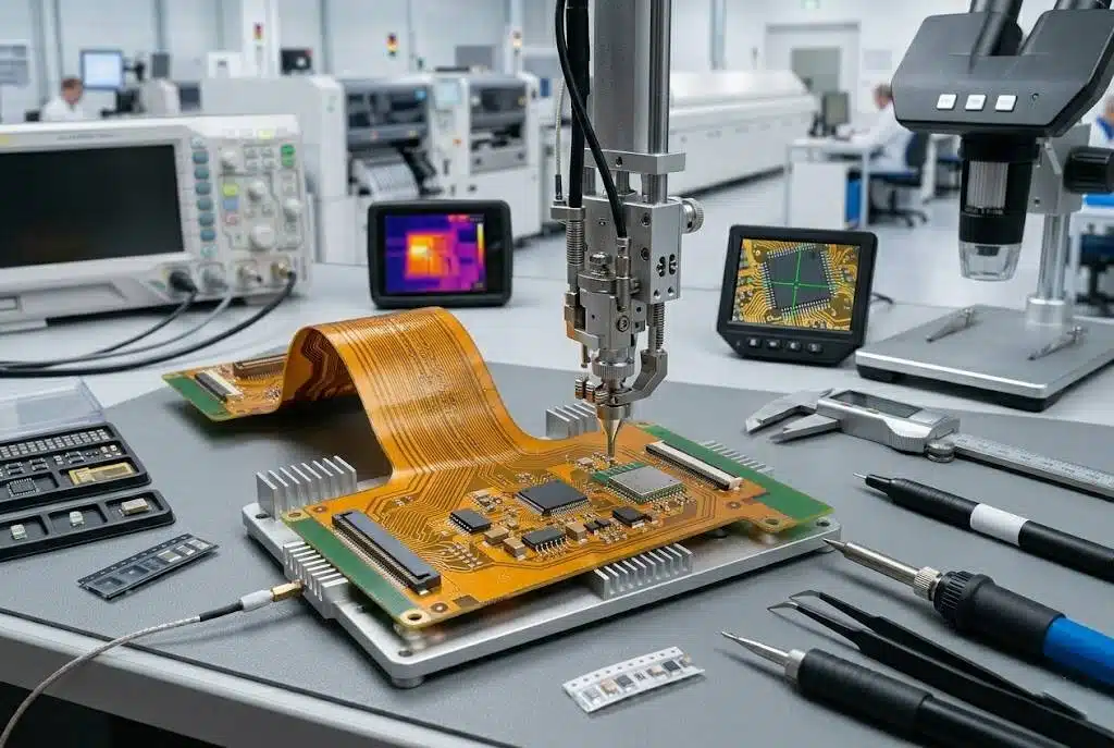
Mixing the two technologies on one board is normal, but the layout has to respect the process. Through-hole parts are typically placed on the primary side so that wave soldering does not have to hold parts in place on the secondary side, and the hole count is kept low to control cost.
Choosing the Substrate
Substrate selection follows the mechanical and thermal requirement rather than the electrical one at these layer counts. FR-4 is the default for general electronics, offering adequate dielectric performance, good mechanical strength, and a wide operating temperature range. Aluminum substrates are used where the board itself must act as a heat spreader, which is common in LED lighting and in power conversion. Flexible materials appear where the board must bend to fit an enclosure, and they bring their own assembly constraints.
Where a product will operate in a humid or contaminated environment, the substrate choice is paired with conformal coating or potting rather than with a more exotic laminate. Surface protection usually solves the environmental problem at lower cost than a material change.
Layout Rules That Apply to Both
Two-layer layouts benefit from a few habits that are easy to apply. Keep the ground distribution as continuous as the routing allows, using the secondary side as a partial plane rather than as a second signal layer where possible. Route power on dedicated wide traces rather than borrowing signal paths. Keep copper away from the board edge by the same margins required at higher layer counts, and maintain adequate spacing between traces that carry switching currents and those that carry sensitive signals.
Where the design is cost-sensitive, the biggest gains come from reducing the number of distinct features rather than from shrinking the board. Fewer drill sizes, a single surface finish, standard panel dimensions, and a component placement that allows a compact panel array all reduce cost more than a marginal reduction in board area.
Common Applications
Single-sided boards are still the right answer for calculators, power supplies, solid-state relays, simple lighting controllers, and products where the circuit is essentially a collection of independent functional blocks. The low component count and generous spacing make these boards easy to inspect and easy to repair, which matters in cost-driven markets.
Double-sided boards cover the next tier: LED lighting assemblies, HVAC controls, vehicle instrument panels, vending machines, industrial sensors, and consumer appliances. These products generally need a ground reference, a moderate component count, and at least some routing that must change sides, which is precisely the point where a second copper layer pays for itself.
When to Move to Four Layers
The decision to move beyond two layers is driven by three signals. The first is a routing completion problem that persists after the placement has been optimized. The second is a signal integrity or emissions requirement that needs a continuous reference plane under fast signals. The third is a power distribution requirement that cannot be met by traces of a practical width.
Any one of these justifies evaluating a four-layer stackup, and the cost difference is often smaller than expected once the savings in area, jumpers, assembly steps, and shielding are accounted for. Layer count choices for simple products are discussed in layer stackup from one to eight layers. The electrical fundamentals of the board itself, including how the copper layers and the substrate interact, are covered in the PCB circuit board explained.
Where cost pressure is severe, there are ways to improve signal behavior on a two-layer design without adding layers, including narrowing the loop area of critical traces and keeping return paths directly beneath their signal traces. These techniques are collected in low-cost signal quality improvements.
FAQ
Can a double-sided board be used without plated holes? It can, but the two sides then have to be connected by soldered wires, rivets, or press-fit pins, which is slower and less reliable than plating. For any product beyond a prototype, plating is the practical choice.
Is a single-sided board suitable for high-frequency circuits? Generally no, because there is no continuous reference plane to define the return path, and the routing detours forced by the single copper layer add inductance. A two-layer board with a partial ground plane is the minimum practical construction for anything with fast edges.
How do I know when the jumper count has become excessive? Treat more than a few zero-ohm links as a signal that the layout is fighting the layer count. At that point the added assembly operations, the board area consumed by the jumpers, and the reliability risk of hand-installed parts usually cost more than the second copper layer.