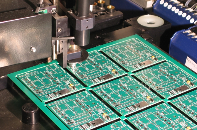
PCB Waste Water Treatment on Site: What Buyers and Engineers Should Check Electronics manufacturing has become a discipline of small details. Solder paste volumes, placement accuracy, temperature profiles and inspection limits all add up to the final result. This guide looks at PCB waste water treatment on site from the…
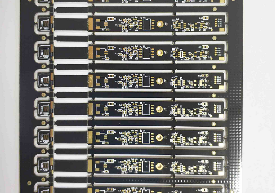
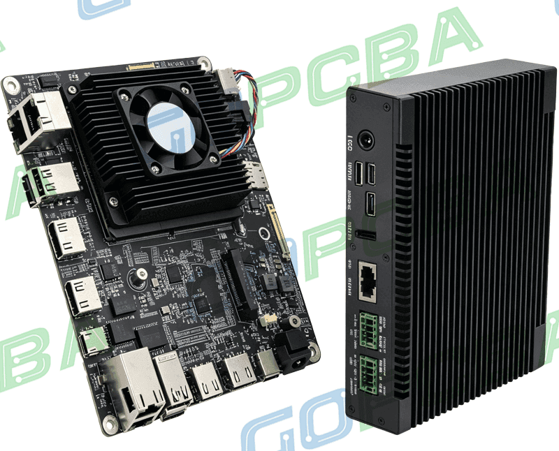
AIoT Processor Core Board Design Considerations A modern processor for embedded vision and edge computing packs eight or more cores, a graphics engine, a neural accelerator and a set of high-speed peripherals into a package that may have a thousand balls at a pitch below a millimetre. The core board…
PCB Chemical Storage and Labelling: Design, Process, and Quality Notes Electronics manufacturing has become a discipline of small details. Solder paste volumes, placement accuracy, temperature profiles and inspection limits all add up to the final result. This guide looks at PCB chemical storage and labelling from the perspective of a…
PCB Scrap and Waste Handling: A Practical Manufacturing Guide Buyers and engineers often focus on the finished product and forget the production line behind it. In practice, most field failures can be traced back to process decisions made during assembly. Understanding PCB scrap and waste handling gives you a practical…
PCB Material Declaration Collection: A Practical Manufacturing Guide Electronics manufacturing has become a discipline of small details. Solder paste volumes, placement accuracy, temperature profiles and inspection limits all add up to the final result. This guide looks at PCB material declaration collection from the perspective of a PCBA factory floor,…
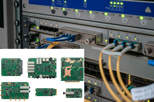
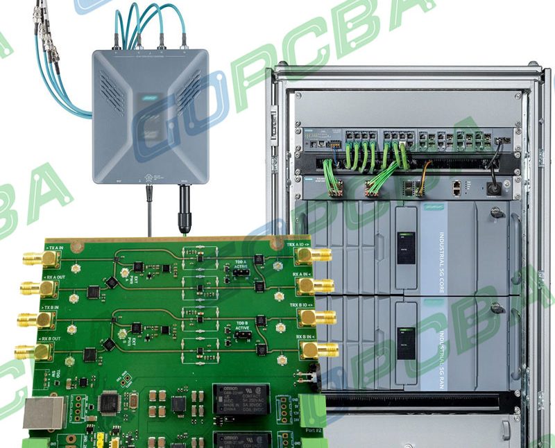
FPGA Board Design for High Speed Interfaces An FPGA is not simply a large component. It is a system on a package, with dozens of high-speed serial channels, several parallel memory interfaces and a power demand that changes faster than any regulator can respond to. The board that carries it…
Via in Pad or Plated Through: Choosing by Cost Placing a via directly in a component pad is a technique that solves a real problem and creates a real cost. It shortens the connection from a fine-pitch device to the inner layers and it frees routing space on the surface,…
PCB RoHS Documentation for A Build: A Practical Review for Manufacturing Teams Buyers and engineers often focus on the finished product and forget the production line behind it. In practice, most field failures can be traced back to process decisions made during assembly. Understanding PCB RoHS documentation for a build…
PCB REACH Compliance for Materials: What Is Restricted Electronics manufacturing has become a discipline of small details. Solder paste volumes, placement accuracy, temperature profiles and inspection limits all add up to the final result. This guide looks at PCB REACH compliance for materials from the perspective of a PCBA factory…
PCB Conflict Minerals Declaration: Where the Metal Came From Modern electronics depend on boards that are assembled correctly the first time. Every product – a phone, a charger, a medical instrument or an industrial controller – relies on thousands of solder joints that must conduct current for years. This article…