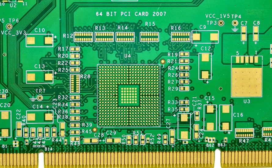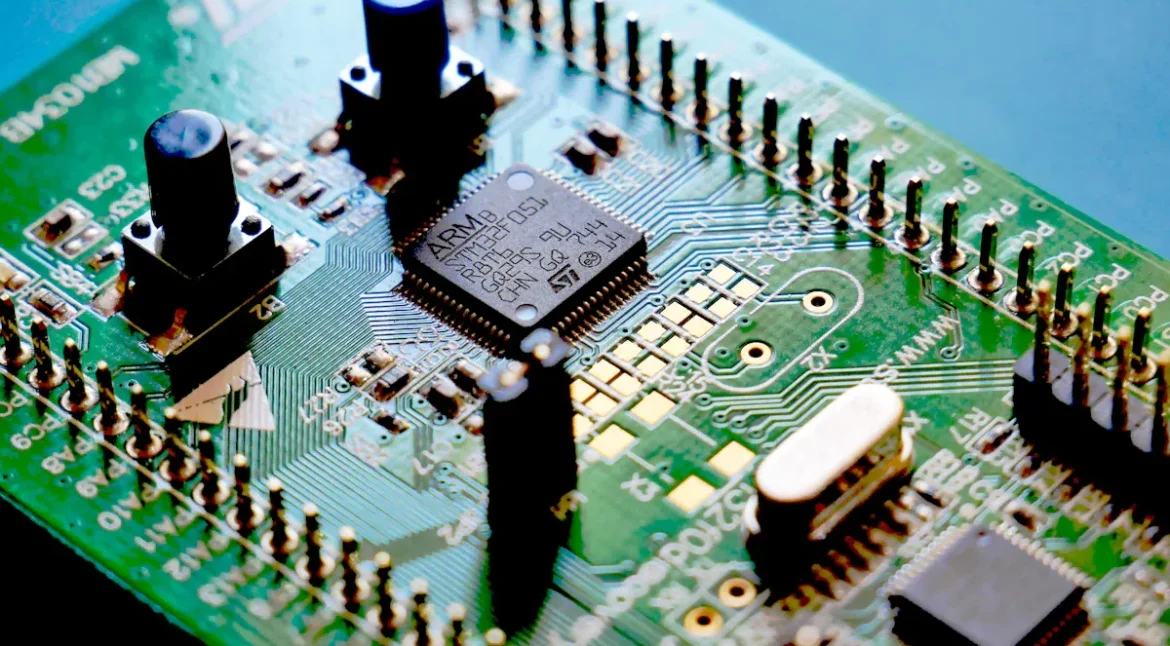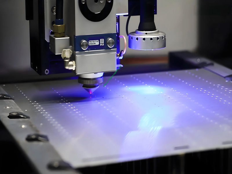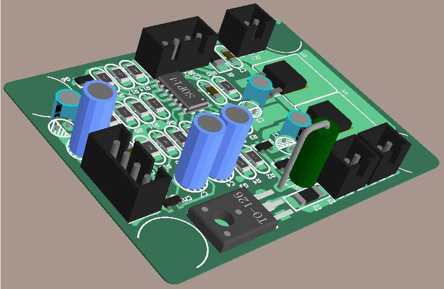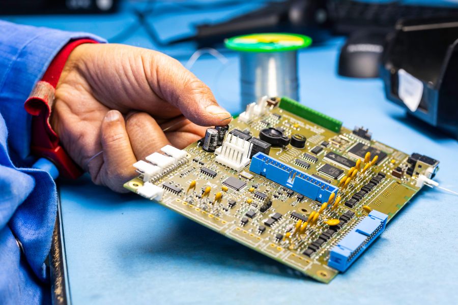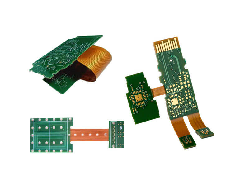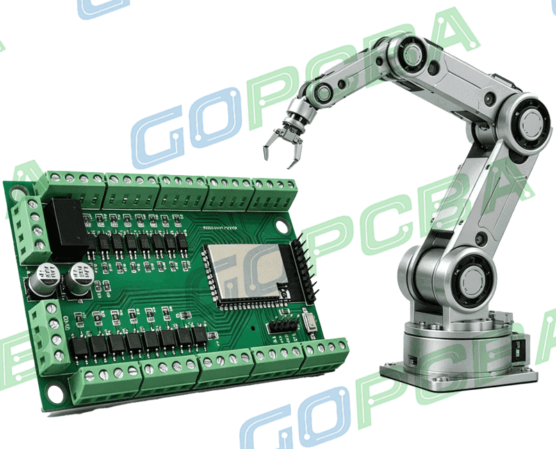
PCB Backdrilling for High Speed: Removing the Stub Electronics manufacturing has become a discipline of small details. Solder paste volumes, placement accuracy, temperature profiles and inspection limits all add up to the final result. This guide looks at PCB backdrilling for high speed from the perspective of a PCBA factory…
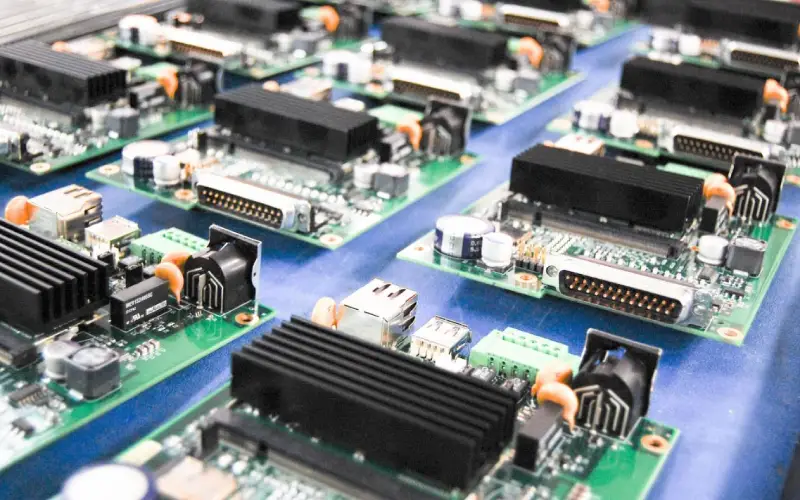
Routing Priority and Crosstalk Control in PCB Layout Routing that begins before the board has been thought about produces work that has to be undone. The usual sequence is familiar: power and general signals are routed first, and somewhere in the middle of the board a group of high-speed nets…
PCB Edge Plating: Metal on the Side Wall Buyers and engineers often focus on the finished product and forget the production line behind it. In practice, most field failures can be traced back to process decisions made during assembly. Understanding PCB edge plating gives you a practical advantage when you…
HDI Layout: Shrinkage Compensation and Microvia Rules High density interconnect changes the questions a layout has to answer. On a conventional board the constraint is usually space: how to fit the routing into the area available. On an HDI board the constraint becomes agreement — between the stack-up and the…
Stepped Substrate Impedance Matching for Millimetre-Wave Boards As frequencies move into the millimetre-wave range, board construction stops being uniform. A design may transition from a very thin core to a standard laminate, from one dielectric constant to another, or from a package substrate down onto the board through an interposer.…
PCB Shipping Protection: Getting It There Intact Electronics manufacturing has become a discipline of small details. Solder paste volumes, placement accuracy, temperature profiles and inspection limits all add up to the final result. This guide looks at PCB shipping protection from the perspective of a PCBA factory floor, covering packing…
Padless Via Design for High-Density Interconnect Every via in a conventional board carries a pad: a ring of copper around the drilled hole that exists to absorb the tolerance between where the hole was drilled and where the circuit expects it. That ring is a design compromise, and at high…
High-Speed FPGA PCB Design: Stack-Up, Power and SerDes A modern high-speed FPGA is not a component that gets placed on a board; it is a system that imposes requirements on everything around it. Transceiver lanes run at tens of gigabits per second, the device may present dozens of them, and…
PCB Moisture Sensitivity Handling: Baking Before Use Electronics manufacturing has become a discipline of small details. Solder paste volumes, placement accuracy, temperature profiles and inspection limits all add up to the final result. This guide looks at PCB moisture sensitivity handling from the perspective of a PCBA factory floor, covering…
Eight DFM Principles for PCBA Assembly Design rules for assembly are not a list of prohibitions. They are the accumulated answers to a simple question: what does the assembly process find easy, and what does it find difficult? The eight principles below are the ones that pay back most often,…