
Routing Priority and Crosstalk Control in PCB Layout
Routing that begins before the board has been thought about produces work that has to be undone. The usual sequence is familiar: power and general signals are routed first, and somewhere in the middle of the board a group of high-speed nets turns out to have no clean path, no consistent layer and no continuous reference. Correcting that means disturbing the routing already placed, and the second attempt is rarely as tidy as the first.
The alternative is a short planning step that fixes the order of work and the rules each net has to satisfy before any of them are drawn.
Setting the Routing Priority
The order of work follows from what is difficult, not from what is convenient.
Critical nets come first: power distribution, small analogue signals, high-speed differential and single-ended nets, clocks and synchronous signals. These are the nets whose requirements cannot be met by whatever space is left over, and once they are placed the remaining room is a known quantity rather than an assumption.
The second principle is to start where the design is densest. Beginning with the device that has the most connections and the tightest area gives the routing the space it needs; beginning elsewhere and arriving at that device later usually means arriving with no space left.
Clocks, high-frequency nets and sensitive analogue signals deserve dedicated layers where the stack-up allows it, along with the smallest practical loop area, adequate clearance and, where necessary, shielding between them and the rest of the design.
And any net with an impedance requirement belongs on a layer whose stack-up was designed to produce that impedance. Reference plane continuity is part of the same requirement: a controlled-impedance net that crosses a split in its reference plane loses the very property the stack-up was built to provide.
Crosstalk and the 3W Rule
Crosstalk is the coupling of energy from one net into another through the capacitance and inductance between parallel conductors. It grows with the length over which two traces run alongside each other, with how close they are, and with how fast the signal is.
The usual spacing guideline is expressed as a multiple of trace width rather than as an absolute distance, because what matters is the ratio of spacing to the geometry that produces the field. Keeping the centre-to-centre spacing at three times the trace width removes most of the electric field coupling between the two lines, which is where the common form of the rule comes from.
Three countermeasures are used, in this order of practicality. Increase the spacing, which costs area and is the simplest. Insert a grounded trace between the aggressor and the victim, which consumes a trace channel but provides shielding. And reduce the distance between the signal layer and its reference plane, which tightens the field around each trace and reduces the coupling it can produce at any given spacing. The last one is a stack-up decision and therefore needs to be made early, since it is effectively free once the layer thicknesses have been chosen.
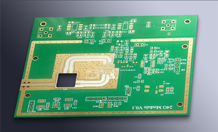
Adjacent Layers Should Run Orthogonally
Two signal layers separated by only a thin dielectric couple into each other, and the coupling is strongest when their traces run parallel on the two layers. Routing adjacent layers in orthogonal directions — horizontal on one, vertical on the next — means the traces cross rather than run alongside, and the coupled length is reduced to the width of the crossing.
Where the construction makes this impossible, as it does on some backplanes, the remedy is to separate the layers with a plane or to run grounded guard traces between the sensitive conductors.
Small Parts and Fine-Pitch Pads
Two-terminal passive components are often routed as an afterthought, and the result is asymmetry. A resistor whose two terminals are connected by traces of different width, or approached from different directions, will heat unevenly during soldering, and a chip component that heats unevenly is a candidate for standing on one end. Symmetric connections at both terminals are the rule.
Fine-pitch surface mount pads have a related requirement: the trace should leave the pad from its outer end rather than from the middle. A trace leaving the centre of a pad divides the paste deposit and leaves the joint with less solder on the side where the fillet has to form.
Keep the Loop Small
A signal and its return path form a loop, and the area of that loop determines both how much interference the circuit radiates and how much it receives. The return path is not a design choice the router makes freely; it follows the reference plane beneath the trace, so the practical rule is to keep high-speed traces close to a continuous plane and to avoid anything that pushes the return current away from directly beneath the trace.
Slots, plane splits and connector areas where the plane is interrupted are the places where loops grow without the trace geometry changing at all.
No Stubs
A stub is a length of trace connected to a net at one end only. It behaves as an unterminated transmission line, and it both radiates and resonates. On fast nets a stub of a few millimetres is enough to degrade a signal, which is why the rule is to eliminate them rather than to shorten them. The places they appear are predictable: test points added late, nets that were rerouted and left a fragment behind, and unused pins that were connected to a net for convenience.
Consistent Trace Width
A net should keep one width along its length. Every change in width is a change in impedance, and a change in impedance is a reflection: the signal sees a discontinuity at each variation, and on a fast net the cumulative effect is a degraded edge and a worse eye.
Some changes cannot be avoided. The trace leaving a fine-pitch package or a connector is narrower than the trace in the open field, because the pitch leaves no alternative. In those cases the goal is to make the narrow section as short as possible, so that the inconsistent portion does not add significant electrical length.
Self-Loops Between Layers
In multilayer designs a net can be routed such that it passes through a layer and then returns to that layer in a way that closes a loop on itself. The loop is an antenna, and it radiates the signal it carries. These are difficult to see on a single layer and are usually found by inspecting the net as a whole rather than layer by layer, which is a reason to review critical nets as complete routes before the layout is released.
Angles
Acute and right angles are avoided for two reasons. Electrically, a sharp corner presents a local change in geometry that reflects part of a fast signal and concentrates field at the point, which is both a loss and a small radiator. In manufacture, an acute corner is difficult to etch uniformly; the etchant tends to over-etch the point, and acid traps form in the narrow angle.
Forty-five degree and curved routing avoid both. Where a corner is unavoidable, a small chamfer removes the electrical and processing problem at the cost of a few tenths of a millimetre.
Working Order
The practical sequence that emerges is: decide the stack-up with the impedance and reference requirements in mind; place the parts so the dense devices have room; route the critical and the densest nets first; keep adjacent layers orthogonal; apply spacing rules that suit the rate the net carries rather than applying one rule everywhere; and check the finished nets for stubs, width changes and loops before releasing the data.
Most of the rules above exist to manage one underlying quantity, which is the field a trace produces and receives. What a reflection does to a signal, and why a width change or a plane split causes one, is described in the note on the reflection coefficient and impedance. The behaviour of fast nets in a crowded layout is covered in the article on high-frequency routing, and the review that catches what the routing has missed is set out in the layout quality checklist.
FAQ
Why is the spacing rule expressed as a multiple of trace width? Because the coupling depends on the relationship between the spacing and the geometry that produces the field. On a narrower trace the same absolute spacing gives better isolation, and on a wider trace it gives worse.
Is a short stub acceptable? Its effect scales with length and with the rate of the signal. On fast nets the accepted length is short enough that the design is usually cleaner without any stub at all.
Should every net follow the same spacing rule? No. Applying the strictest rule everywhere wastes area on nets that do not need it and can force routes onto worse paths. The rule should follow the rate of the net.