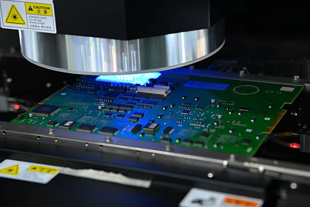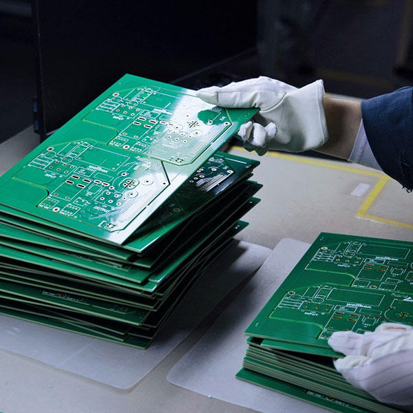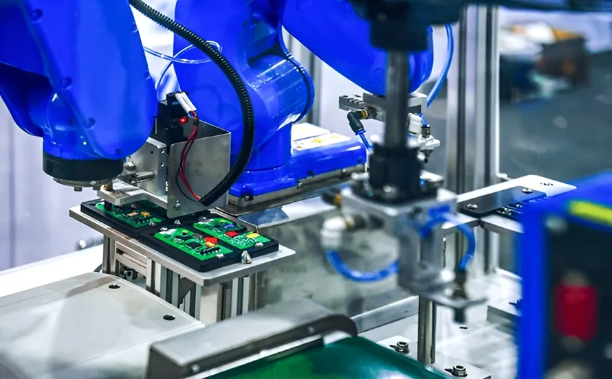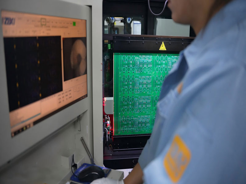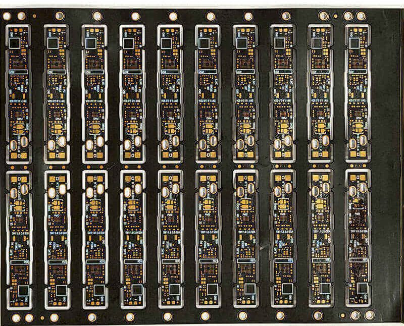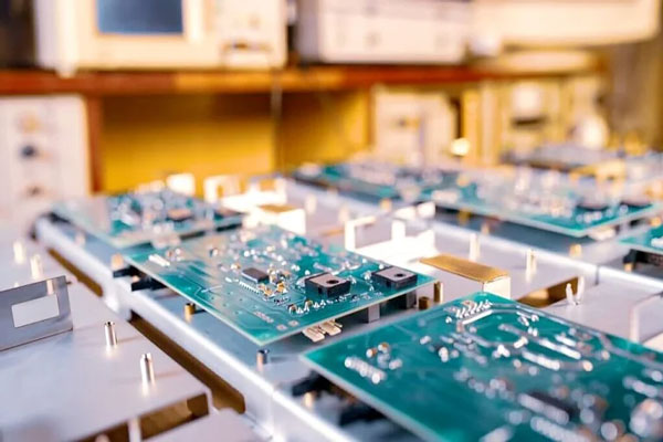
How a Placement Factory Keeps Product Quality Consistent Electronics manufacturing has become a discipline of small details. Solder paste volumes, placement accuracy, temperature profiles and inspection limits all add up to the final result. This guide looks at PCB placement factory product quality from the perspective of a PCBA factory…
ABF PCB Substrate: 20-Layer Structure, Materials and Cost Guide What Is an ABF PCB Substrate? An ABF PCB substrate is a high density IC package substrate built with Ajinomoto Build-up Film, the ABF dielectric that enables the finest line widths and smallest laser vias in advanced semiconductor packaging. The substrate…
Material Requirements at a PCB Placement Factory Electronics manufacturing has become a discipline of small details. Solder paste volumes, placement accuracy, temperature profiles and inspection limits all add up to the final result. This guide looks at PCB placement factory material requirements from the perspective of a PCBA factory floor,…
What a Normal Defect Rate Looks Like in PCB Placement Electronics manufacturing has become a discipline of small details. Solder paste volumes, placement accuracy, temperature profiles and inspection limits all add up to the final result. This guide looks at PCB placement factory defect rate from the perspective of a…
Comparing PCB Manufacturers on Quality, Not Just Price Modern electronics depend on boards that are assembled correctly the first time. Every product – a phone, a charger, a medical instrument or an industrial controller – relies on thousands of solder joints that must conduct current for years. This article explains…
PCB Solder Mask Touch-Up: The Complete Repair Guide What Is PCB Solder Mask Touch-Up? PCB solder mask touch-up, sometimes called solder mask repair or spot solder mask application, is the process of repairing small local defects in the solder mask layer without rebuilding the whole board. During fabrication, handling, SMT…
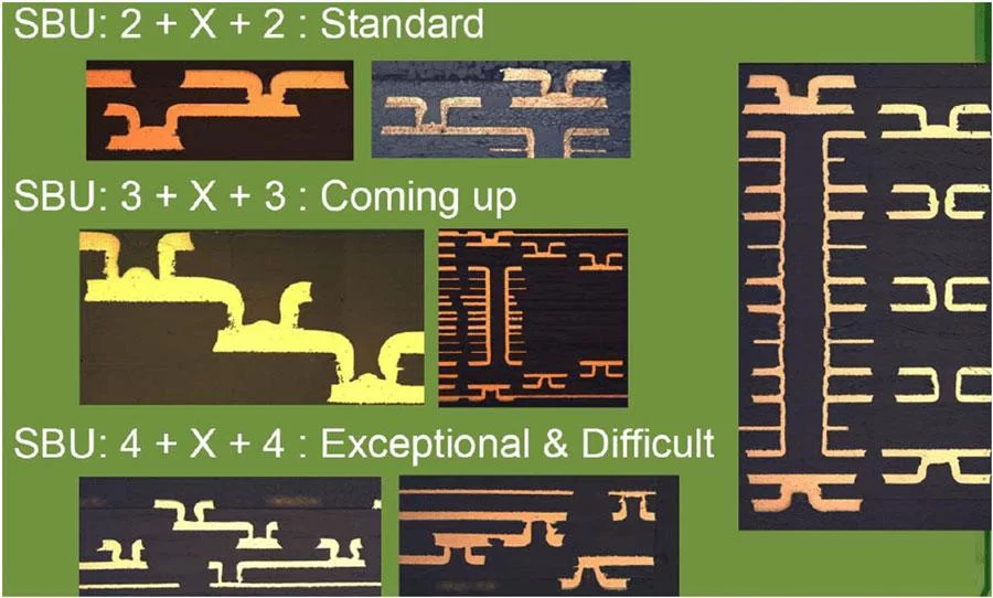
Buried Via vs Microvia PCB: Full Comparison Guide Buried Vias and Microvias at a Glance Modern PCB design keeps packing more function into less space, and the wiring between layers is where the fight is won. Two advanced interconnection techniques do most of the work: buried vias, which connect inner…
Laser-Cut vs Electroformed PCB Stencil: Which Is Better? What Is a PCB Stencil? A PCB stencil, also called an SMT stencil or solder paste stencil, is the tool that decides how much solder paste lands on every pad of a board. The stencil is normally stainless steel or nickel with…
Semiconductor Test Burn-in Board: The Complete Guide What Is a Semiconductor Test Burn-in Board? A semiconductor test burn-in board is a high reliability PCB that sits between a device under test and the burn-in oven or automatic test equipment used to qualify chips. Each board carries a number of test…
Dog Bone vs Via-in-Pad PCB: Which BGA Fan-Out Design Is Better? What Are Dog Bone and Via-in-Pad Fan-Out? Every PCB that carries a fine-pitch BGA package faces the same question at the layout stage: how do we break the hundreds of solder balls out to the inner layers and the…