Buried Via vs Microvia PCB: Full Comparison Guide
Buried Vias and Microvias at a Glance
Modern PCB design keeps packing more function into less space, and the wiring between layers is where the fight is won. Two advanced interconnection techniques do most of the work: buried vias, which connect inner layers without touching the board surface, and microvias, tiny laser-drilled holes that usually connect adjacent layers. Both raise routing density compared with ordinary through holes, but they are built differently, cost differently and perform differently.
Buried vias are drilled mechanically inside the layer stack before lamination, so they disappear once the outer layers are added. Microvias are laser-drilled into the outer surface of each build-up layer and are the core technology of HDI printed circuit boards. Choosing between them is not about which is better in the abstract; it is about matching the via strategy to the layer count, signal speed, density and budget of the actual design.
This guide compares the structure, manufacturing flow, electrical and thermal behavior, cost, applications and standards of buried via and microvia boards.
What Is a Buried Via PCB?
A buried via connects two or more internal conductive layers and is completely invisible from the outside of the board. Because it never reaches the surface, it frees the outer layers for component placement and routing, which improves the wiring efficiency of multilayer boards without adding surface via congestion.
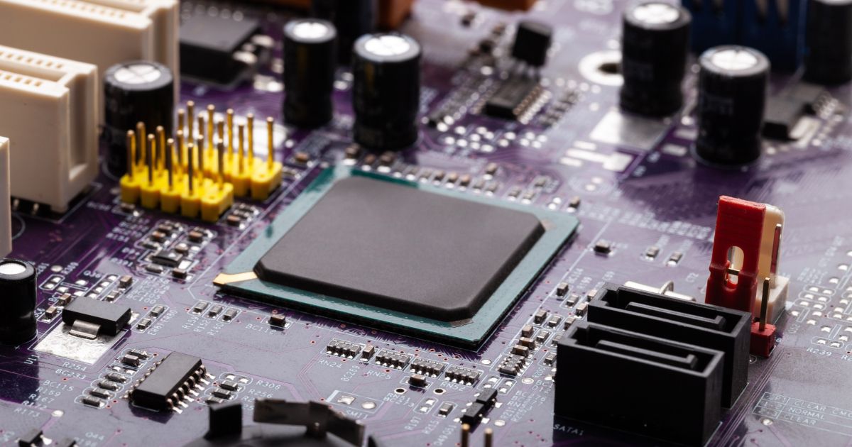
Buried vias are produced by drilling and plating the inner layers before they are laminated into the final stack. Typical hole sizes range from 0.15 to 0.30 millimeters, processed with mechanical drilling and copper plating, and the construction suits boards from six layers upward, with aspect ratios up to roughly ten to one depending on the factory’s capability. They are a mature, reliable way to route high layer count boards for networking, data center, automotive and industrial applications.
What Is a Microvia PCB?
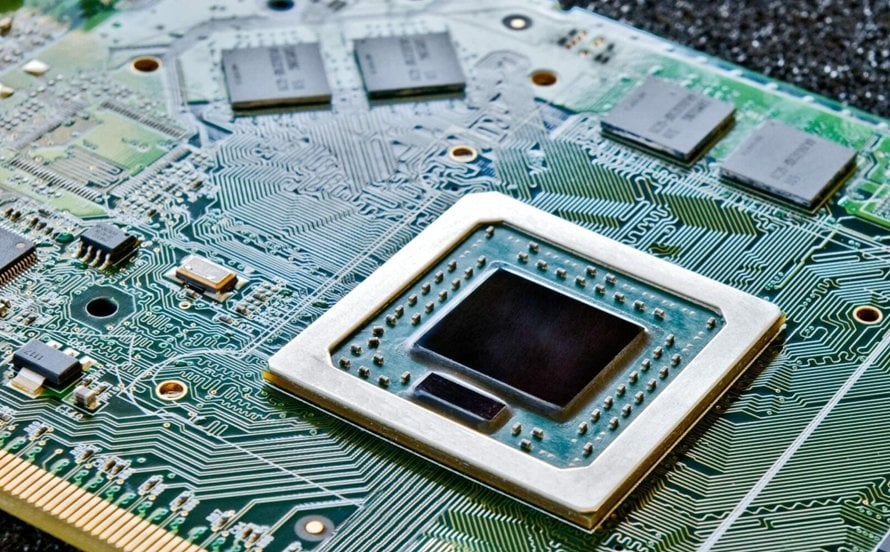
A microvia is a very small hole, usually 50 to 150 micrometers in diameter, created by laser drilling rather than mechanical drilling. Standard microvias connect two adjacent layers, and by stacking or staggering them, designers can reach across several layers of an HDI structure. The tiny size and short connection path make microvias the preferred fan-out for fine pitch BGA packages and the foundation of compact, high performance products.
Microvia boards rely on sequential lamination: each build-up layer is drilled, plated, and often filled with resin or copper before the next layer is added. Because the hole walls are short, the aspect ratio stays low, typically below one to one, which keeps plating reliable. Stacked and staggered microvias give HDI boards their characteristic high density, and filled vias under BGA pads double as thermal paths.
Structure and Process Differences
The structural difference is easy to state. Buried vias live between internal layers, are drilled mechanically at a relatively large size and connect layers that are already part of the inner core. Microvias are laser-drilled from the surface of each sequential build-up layer, are extremely small, and are typically filled before the next lamination step.
The process flows are equally different. A buried via board follows inner layer imaging, inner layer drilling, hole plating, inner AOI, lamination, outer drilling, panel plating and finishing. A microvia HDI board cycles through core fabrication, laser drilling, desmear, copper deposition and plating, via filling, build-up lamination, another laser drilling pass and so on until the outer layers are formed. Every extra build-up cycle adds process steps, alignment challenges and cost, which is why microvia boards are harder to build than buried via boards.
Routing Density and Electrical Performance
Buried vias improve density by removing through holes from the surface and giving inner layers more room, which is valuable on mid to high layer count boards. Microvias take density much further because their tiny size lets designers route between closely spaced BGA balls and shrink the overall footprint, which is exactly why smartphones, AI compute modules and wearables depend on them.
Electrically, microvias usually win on high speed signals. Their stub length is essentially zero, and their small size lowers parasitic capacitance and inductance compared with larger buried or through vias. That makes them ideal for PCIe, DDR5, USB4, 112G SerDes and high speed switch applications where every parasitic element distorts the signal. Buried vias still outperform plain through holes because their shorter path reduces reflection and keeps impedance control tighter, which matters in high speed digital circuits that do not need full HDI density.
Thermal Performance and Reliability
Both via types help move heat, but in different ways. Buried vias spread heat through internal copper planes across the board, improving overall thermal distribution. Copper-filled microvias create a direct thermal path from a hot BGA pad down to the inner copper, which gives excellent local heat spreading under processors, power ICs and RF devices. High power designs typically combine both with dedicated thermal via arrays.
Reliability depends on process maturity. Buried via technology is long established, and its larger holes with thicker copper deliver excellent long term reliability in demanding environments. Microvia reliability has improved steadily as laser drilling, copper filling and HDI lamination matured; built to IPC standards, stacked microvia structures satisfy automotive, medical and industrial requirements, though design rules such as limiting the number of stacked vias should still be respected.
Cost Comparison
Cost scales with the number of process steps. For prototypes of one to ten boards, a buried via PCB typically quotes between 300 and 900 US dollars, while a microvia HDI board, with its laser drilling, multiple laminations and via filling, usually runs 600 to 2000 dollars. In small batch production of fifty to five hundred boards, buried via boards commonly land at 40 to 180 dollars per board and microvia boards at 70 to 350 dollars per board. At volumes above one thousand boards, unit costs fall sharply for both, but the microvia premium remains because the process itself is longer.
The deciding question is whether the extra density and electrical performance of microvias save enough elsewhere, such as a smaller board size or fewer layers, to offset the higher fabrication cost. On high end products they usually do; on cost driven designs, buried via routing is frequently the more sensible choice.
Typical Applications
Buried via boards appear in industrial control equipment, networking hardware, data center server motherboards, automotive ECUs, medical electronics, aerospace systems and power control equipment, where high layer counts and long term reliability matter more than absolute miniaturization. Microvia HDI boards dominate smartphones, AI server accelerator cards, GPU boards, high performance computing, wearables, AR and VR devices, solid state drives, 5G modules and defense electronics, where density and signal speed are everything.
IPC Standards
Both technologies are governed by the IPC family of standards. IPC-2221 covers general PCB design, while IPC-2226 addresses HDI design specifically. IPC-6012 sets the performance specification for rigid boards, IPC-6016 covers HDI boards, IPC-A-600 defines acceptance criteria, and IPC-6018 applies to high frequency boards. Following these standards keeps the product consistent, reliable and stable over its operating life, and high reliability buyers should confirm the factory’s class rating before placing orders.
DFM Advice for Via Selection
A few design habits prevent most via related problems. Use buried vias only where they add real value, because every extra hole type complicates the build. Choose microvias for ultra fine pitch BGA fan-out. Keep stacked microvia levels to a minimum for reliability. Design adequate annular rings so drill misregistration does not break the connection. Respect the aspect ratio limits of the manufacturer, balance copper across layers to limit warpage, and for high speed designs evaluate impedance, return paths and via stubs together rather than in isolation.
Running a DFM review with the factory early in the design cycle is the cheapest insurance, because via strategy affects stack-up, tooling and cost from the very first layout decisions.
FAQ
Is a buried via PCB better than a microvia PCB? Not absolutely. Buried vias suit high layer count boards where mature, reliable inner layer routing is needed, while microvias suit HDI designs, high speed signals and dense packaging. The right answer depends on the design.
Why is microvia PCB pricing higher? Microvia boards require laser drilling, sequential lamination and via filling, all of which add equipment time and process risk compared with the mechanical drilling used for buried vias.
Can microvias and buried vias be combined? Yes. Many advanced multilayer boards mix buried vias in the core with microvia build-up layers to balance density, signal performance and cost in one stack-up.
Manufacturing Both Via Types Well
The value of advanced via technology only appears when the factory can execute it reliably. Look for a manufacturer with high layer count capability above sixty layers, buried and blind via processing, laser microvias and copper filling, HDI builds from one plus N plus one upward, sequential lamination, and experience with high speed materials such as Rogers, Megtron, Isola and Panasonic laminates under precise impedance control and IPC Class 2 or Class 3 programs.
gopcb manufactures high layer count, HDI and high reliability PCBs with buried via and stacked or staggered microvia capability, offering DFM review, prototype through production volumes and fast delivery for AI, automotive, medical and industrial customers. Send your stack-up and via plan for a free manufacturability assessment and a quotation built on the real process.