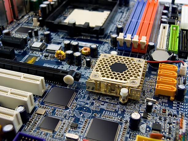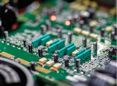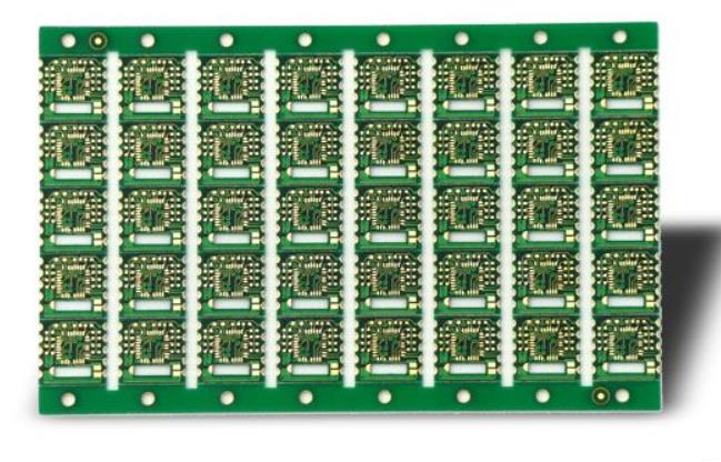
Custom Wireless Charging PCB Guide | Lead Time, MOQ & Price December 29, 2025 · Posted by gopcbadmin As wireless charging technology moves from premium features to mainstream adoption across consumer electronics, automotive, and industrial sectors, the wireless charging PCB has become the critical backbone of modern wireless power systems.…
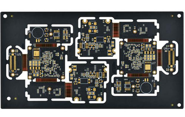
VIPPO PCB Ordering Guide: Design Rules, MOQ & Lead Time December 31, 2025 As electronics continue to evolve toward miniaturization, high integration, and superior reliability, PCB designs face escalating demands for BGA pad density, signal integrity, and assembly yield. Traditional through-hole or resin-plugged via solutions increasingly reveal soldering defects and…
Low Cost PCB Supplier China: Cost Breakdown & Order Guide 06 Jan In the global electronics manufacturing industry, low-cost PCB suppliers in China have become the preferred choice for countless engineers, procurement managers, and hardware startups. A true low-cost PCB is not a “cheap circuit board” that compromises quality; rather,…
Medical PCB Prototype & Production Services September 5, 2026 · Shenzhen In the medtech field, reliability, safety, and legal compliance are non-negotiable. Whether for patient tracking, medical imaging, or wearable devices, the medical PCB is the critical foundation for stable system operation. Medical PCB sampling and volume production services bridge…
18-Layer PCB Complete Technical Guide for Engineers 13 January · In today’s rapidly evolving electronics industry, multilayer PCBs are the backbone of high-performance electronic systems. Among them, 18-layer PCBs are especially critical for uses demanding exceptional signal integrity, compact form factors, and high-density interconnects. From telecommunications infrastructure to data centers,…
High-Frequency Rogers PCB Manufacturing Process Rogers laminates behave differently from FR4, and the process must follow those differences. Low dielectric constant and low loss keep insertion loss small, but only if fabrication protects the material. Signal traces are sensitive to impedance shifts, surface roughness and dimensional movement. A build that…
20 Layer Multilayer PCB Manufacturer: Process Checks A 20-layer board packs ten times the routing of a simple double-sided design into one thin package. That density brings real benefits for signal integrity and thermal spreading. It also brings a long chain of process steps where small errors compound fast. This…
10 Layer Any Layer HDI PCB: Stackup and Process Review A 10 layer any layer HDI board is not simply a thicker multilayer board. Every layer can host laser microvias, so routing freedom rises sharply while the process window narrows. The stackup, the dielectric materials and the via fill all…
How to Reduce Impedance PCB Manufacturing Costs Impedance-controlled boards carry tighter tolerances than standard boards. That tightness shows up in material selection, stackup design, and process control. Each choice adds cost, but not every choice adds value. The goal is to pay for the control the product actually needs. This…
Four Layer PCB Prototype Manufacturing for Fast Turnaround A four layer prototype carries the first real evidence that a design works. The board must arrive quickly, but speed alone proves nothing if the layers drift or the impedance wanders. Buyers therefore need a supplier who can compress the schedule without…