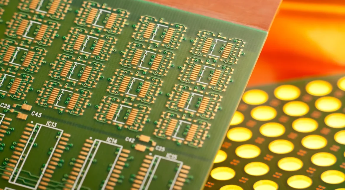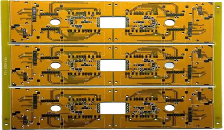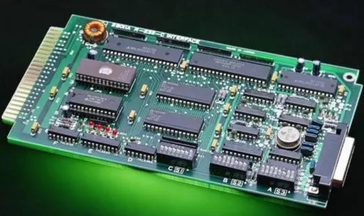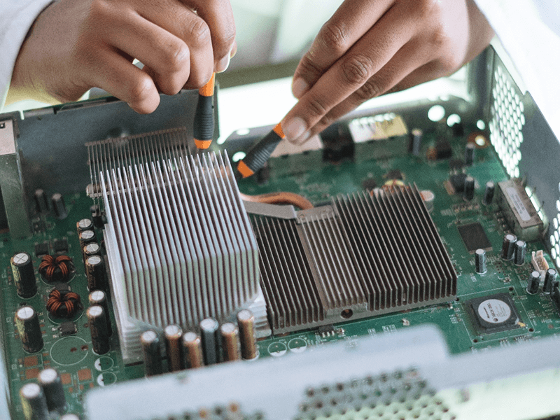
Copper Thieving Pattern Design For Even Etching A thieving pattern is copper added to a layer purely for process reasons. It carries no signal and connects to nothing, yet it changes how the etchant flows, how the plating current distributes, and how the finished panel behaves under heat. On boards…
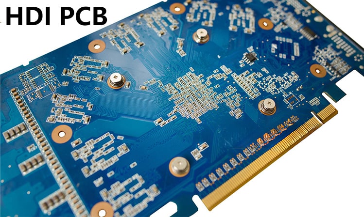
AOI Programming Strategy for Mixed Technology Boards An AOI programme is a measurement routine, not a photograph album. It decides what the machine looks for, how much variation it tolerates and what it reports, and those decisions determine whether the station finds real defects or trains operators to ignore alarms.…
Component Polarity Verification Practice on the SMT Line A reversed diode, capacitor or connector is one of the most expensive assembly defects, because it usually passes electrical test in a way that looks acceptable and fails later in the field. Polarity is decided by conventions that differ between packages, between…
PCB Desmear Process Control For Reliable Hole Walls Drilling a multilayer board generates enough heat to soften the resin, and the bit drags that softened material across the freshly cut hole wall. The resulting smear is a thin, electrically insulating film over the inner layer copper, and if it is…
PCB Shop Humidity Cost: Design and Assembly Considerations Electronics manufacturing has become a discipline of small details. Solder paste volumes, placement accuracy, temperature profiles and inspection limits all add up to the final result. This guide looks at PCB shop humidity cost from the perspective of a PCBA factory floor,…
PCB Shop Humidity Audit: Process Details and Inspection Points Buyers and engineers often focus on the finished product and forget the production line behind it. In practice, most field failures can be traced back to process decisions made during assembly. Understanding PCB shop humidity audit gives you a practical advantage…
PCB ESD Control Plan: Process Details and Inspection Points Electronics manufacturing has become a discipline of small details. Solder paste volumes, placement accuracy, temperature profiles and inspection limits all add up to the final result. This guide looks at PCB ESD control plan from the perspective of a PCBA factory…
Underfill Application Methods for BGA Solder Joint Life Underfill is a filled epoxy that flows into the gap beneath a package and surrounds every solder joint. It does not make a joint stronger in tension, but it changes how the joint responds to thermal cycling by spreading the strain across…
Solder Ball and Solder Beading Control A solder ball is a small sphere of alloy sitting on the board surface, usually beside a joint and often unconnected to anything. Solder beading is a related but distinct defect in which a ball is attached to the side of a joint or…
Stencil Tension and Frame Selection for Fine Pitch Stencil tension is one of the few stencil properties that changes continuously through the life of the tool, and it changes the printed deposit long before anyone notices a defect. A loose stencil flexes away from the board during separation, which smears…