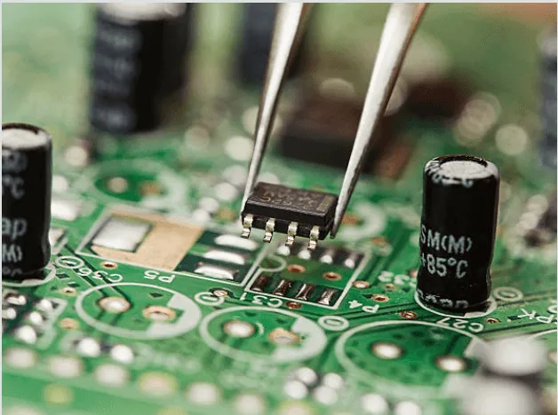
PCB ENIG Finish Improvement: Key Process and Quality Checks Buyers and engineers often focus on the finished product and forget the production line behind it. In practice, most field failures can be traced back to process decisions made during assembly. Understanding PCB ENIG finish improvement gives you a practical advantage…

Component Placement Sequence Optimisation for SMT Assembly Component placement sequence is the order in which a machine places parts on a board, and it is one of the few variables in surface mount assembly that can be changed without touching the design or the process. A well ordered program reduces…
PCB ENIG Finish Selection: From Design to Repeatable Production Buyers and engineers often focus on the finished product and forget the production line behind it. In practice, most field failures can be traced back to process decisions made during assembly. Understanding PCB ENIG finish selection gives you a practical advantage…
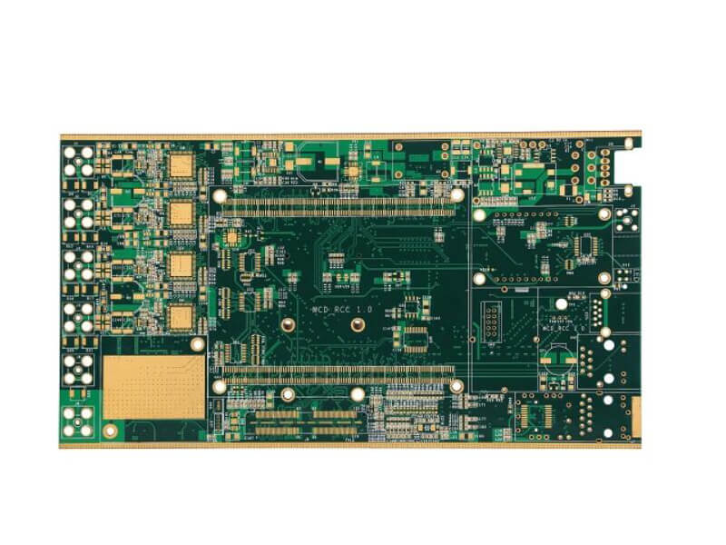
PCB ENIG Finish Timing: Practical Process Controls Buyers and engineers often focus on the finished product and forget the production line behind it. In practice, most field failures can be traced back to process decisions made during assembly. Understanding PCB ENIG finish timing gives you a practical advantage when you…
PCB ENIG Finish Sample: From Design to Repeatable Production Modern electronics depend on boards that are assembled correctly the first time. Every product – a phone, a charger, a medical instrument or an industrial controller – relies on thousands of solder joints that must conduct current for years. This article…
Board Thickness Selection For PCB Designs Board thickness looks like a simple choice, and in most projects it is made by default at 1.6 mm. That figure is a convention rather than a requirement, and the right thickness depends on the mechanical environment, on the connector system and on the…
PCB ENIG Finish Control: What Buyers and Engineers Should Check Modern electronics depend on boards that are assembled correctly the first time. Every product – a phone, a charger, a medical instrument or an industrial controller – relies on thousands of solder joints that must conduct current for years. This…
Solder Mask Dam Design Between Fine Pitch Pads A solder mask dam is the narrow strip of mask that separates two adjacent pads. Its purpose is to stop molten solder from wicking from one pad to the next during reflow, and its width is one of the tightest features on…
Component Rotation Errors In SMT Assembly A component rotation error is a placement that is correct in position but wrong in orientation. The part sits neatly on its pads, so the board can pass a simple positional check, yet the polarity or the pin numbering is reversed and the assembly…
PCB ENIG Finish Traceability: Process Details and Inspection Points Electronics manufacturing has become a discipline of small details. Solder paste volumes, placement accuracy, temperature profiles and inspection limits all add up to the final result. This guide looks at PCB ENIG finish traceability from the perspective of a PCBA factory…