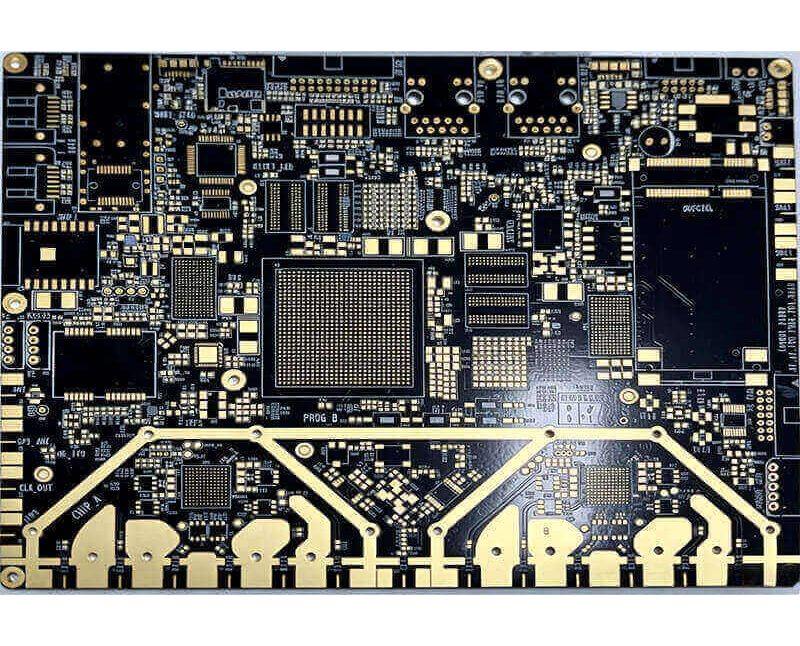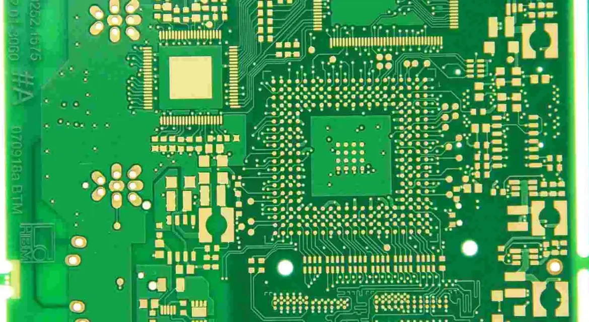
PCB ENIG Finish Problems: From Design to Repeatable Production Electronics manufacturing has become a discipline of small details. Solder paste volumes, placement accuracy, temperature profiles and inspection limits all add up to the final result. This guide looks at PCB ENIG finish problems from the perspective of a PCBA factory…

Creepage And Clearance: Design Rules and Process Limits Creepage and clearance are the two distances that separate conductors held at different potentials. Clearance is the shortest distance through air, and creepage is the shortest distance along the surface of the insulation. Both have to be large enough that the voltage…
Router Bit Selection for Depaneling Routing separates boards from a panel with a rotating bit that follows the outline. It is the most flexible depaneling method, since it can follow any shape and it leaves an edge with no taper, and its quality and its cost both depend on the…
Component Spacing Rules For SMT Layout A component spacing rule defines how close two parts may be placed to each other and to other features on the board. It is written for the process rather than for the circuit, and it exists because assembly equipment, rework tools, heat and inspection…
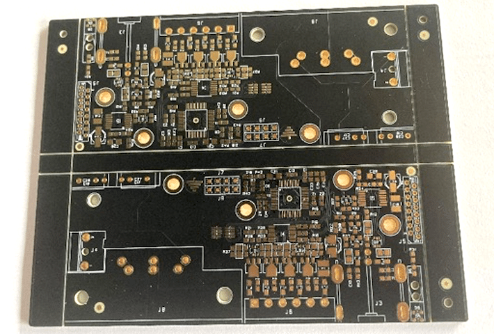
V Cut Scoring Guide for PCB Panels V cut scoring cuts a groove along both faces of a panel so that the boards can be snapped apart later. It is fast, it leaves a clean straight edge and it costs less than routing, and it works only where the boards…
Bare Board Test Strategy for Electrical Continuity Checks A bare board test is an electrical check carried out on the board before any components are fitted, and it exists to catch the faults that no amount of visual inspection can find. The board is finished at that point, with all…
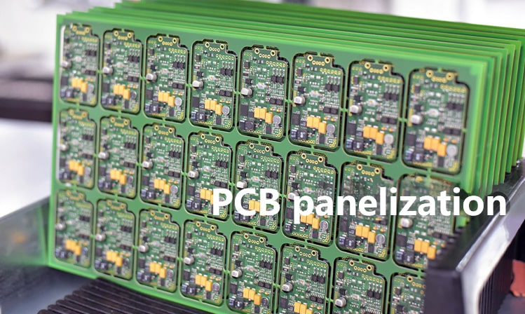
Panelization: Key Checks Before Release Panelization is the arrangement of boards into an array so that they can be processed as one unit. It decides how the boards are held during assembly, how they are separated afterwards and how much of the panel is spent on material that will be…
PCB Warpage After Reflow: Causes and Control Measures PCB warpage after reflow is a change in the flatness of a board caused by the heat of the soldering cycle, and it appears even on boards that were flat when they left the fabricator. The distortion is usually a few tenths…
Panel Size Selection for PCB Fabrication The panel is the manufacturing unit. It is larger than the finished board and it carries the borders, the tooling features and the array of boards that will be separated at the end. Panel size selection is a balance between the amount of material…
Laminate Storage and Handling Guide A laminate and a prepreg are reactive materials. The resin in a prepreg is partly cured and continues to advance slowly at room temperature, and both the prepreg and the finished laminate absorb moisture from the air. Laminate storage is therefore a control on two…