PCB Vias: Types, Drilling Methods, Design Rules, and Via Filling
Vias are one of the most fundamental structures in printed circuit board manufacturing. They provide electrical connections between different PCB layers and allow designers to route signals and power through multilayer circuit boards.
Unlike component holes, vias are primarily designed for interlayer electrical connections rather than component soldering. Depending on their structure and manufacturing method, PCB vias can be classified into through-hole vias, blind vias, buried vias, and microvias.
For complex multilayer and high-density circuit boards, choosing the right via structure is essential for routing density, signal integrity, manufacturability, reliability, and cost.
For projects requiring advanced multilayer structures, you can also review our PCB Manufacturing Services to understand available fabrication technologies and production capabilities.
What Is a PCB Via?
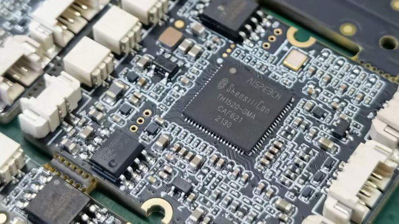
A PCB via is a plated hole that creates an electrical connection between copper layers of a printed circuit board. During PCB fabrication, the hole is drilled or laser-formed and then plated with copper to create a conductive path.
Vias are commonly used to:
- Connect traces between different PCB layers
- Connect signal and power planes
- Provide grounding paths
- Improve routing density
- Reduce PCB size
- Support high-density interconnect structures
- Provide thermal paths in appropriate designs
The correct via structure depends on the PCB layer count, stack-up, component density, signal speed, manufacturing process, and cost requirements.
For advanced circuit boards, via structures are often combined with HDI technology, fine-line routing, and sequential lamination.
Main Types of PCB Vias
There are three traditional via structures: through-hole vias, blind vias, and buried vias. Microvias are also widely used in modern HDI PCB manufacturing.
Blind Vias
A blind via connects an outer PCB layer to one or more inner layers without extending through the entire board.
For example, a blind via can connect Layer 1 to Layer 2 or Layer 3 while remaining inaccessible from the opposite side of the PCB.
Blind vias are particularly useful when designers need to increase routing density without occupying routing space through every PCB layer.
Common applications include:
- Fine-pitch BGA breakout
- HDI PCB designs
- Compact electronic devices
- High-density multilayer boards
- High-speed electronic products
Blind vias require accurate depth control during fabrication. Mechanical drilling must be carefully controlled along the Z-axis, while laser drilling requires precise process parameters.
Improper drilling depth can cause plating problems, insufficient copper coverage, or reliability issues.
For more information about high-density structures, see our HDI PCB Manufacturing resources.
Buried Vias
A buried via connects two or more internal PCB layers without reaching either the top or bottom surface.
Because buried vias are completely enclosed within the PCB structure, they are not visible from the external surfaces of the finished board.
Buried vias can provide additional routing space and are particularly useful for high-density multilayer PCB designs.
Their advantages include:
- More efficient internal routing
- Better utilization of PCB space
- Reduced dependence on outer-layer routing
- Support for complex multilayer designs
- Greater flexibility for high-density interconnections
However, buried vias require additional fabrication processes. The internal layers must generally be drilled and processed before the complete multilayer structure is laminated.
As a result, buried-via PCB fabrication is normally more complex and expensive than conventional through-hole construction.
Designers should therefore use buried vias when their electrical or routing benefits justify the additional manufacturing cost.
Through-Hole Vias
A through-hole via passes through the entire PCB and can electrically connect multiple layers.
The hole is mechanically drilled and copper-plated to create a conductive path through the board.
Through-hole vias are widely used because they are relatively straightforward to manufacture and provide reliable interlayer connections.
Typical applications include:
- Standard multilayer PCBs
- Power connections
- Ground connections
- Signal routing
- Component through-hole connections
It is important to distinguish a via from a component through-hole. A via is primarily intended for electrical interconnection, while a component hole is designed to accommodate a component lead.
Through-hole structures can consume routing space on multiple layers. Therefore, blind vias, buried vias, or microvias may be preferred when board density becomes a major design constraint.
For complete fabrication requirements, explore our PCB Manufacturing Capabilities.
Microvias in HDI PCB Design
Microvias are very small vias, typically produced using laser drilling rather than conventional mechanical drilling.
They are widely used in HDI PCBs because they allow designers to create short vertical connections between adjacent layers while occupying significantly less space than conventional through-hole vias.
Microvias can be configured as:
- Staggered microvias
- Stacked microvias
- Copper-filled microvias
Their compact dimensions make them particularly useful for fine-pitch BGA components, high-density processors, RF modules, smartphones, wearable devices, and other compact electronic products.
However, microvia manufacturing requires precise control of drilling, copper plating, lamination, alignment, and filling processes.
The actual minimum microvia size should always be determined according to the selected PCB manufacturer’s current manufacturing capabilities rather than relying on a universal design rule.
PCB Via Drilling Methods
PCB via fabrication mainly uses two drilling technologies: mechanical drilling and laser drilling.
Mechanical Drilling
Mechanical drilling uses CNC-controlled drill equipment to create holes in PCB materials.
It is commonly used for:
- Through-hole vias
- Component holes
- Larger mechanical holes
- Standard multilayer PCB structures
Mechanical drilling is mature, efficient, and suitable for many conventional PCB designs.
However, mechanical drills have physical limitations when extremely small holes are required. Drill diameter, board thickness, aspect ratio, tool wear, registration accuracy, and material characteristics all influence the achievable result.
Laser Drilling
Laser drilling is commonly used for microvias and advanced HDI structures.
Instead of using a mechanical drill bit, a focused laser removes dielectric material to create very small holes.
Laser drilling provides several advantages:
- Smaller via diameters
- High positional accuracy
- Better suitability for HDI structures
- Efficient processing of microvias
- Improved routing density
The appropriate drilling method depends on the via diameter, layer structure, PCB material, aspect ratio, production volume, and required reliability.
PCB Via Design Rules
Correct via placement is critical to PCB performance and manufacturability. Poorly positioned vias can create electrical interference, routing problems, manufacturing defects, and unnecessary production costs.
Maintain Adequate Clearance
Vias should have sufficient clearance from:
- Components
- Other vias
- Copper traces
- Pads
- Board edges
- Mechanical structures
The exact clearance should be determined according to the PCB manufacturer’s design rules and the specific PCB technology.
Avoid applying one fixed clearance value to every PCB project because manufacturable spacing depends on the PCB process, copper thickness, board structure, and required reliability.
Avoid Unintentional Overlap
Designers should ensure that vias do not unintentionally overlap traces or pads on adjacent layers.
A via passing through an inappropriate copper feature can create an unintended electrical connection or short circuit.
For high-density designs, the PCB stack-up and layer connectivity should therefore be reviewed carefully before routing is finalized.
Consider Current-Carrying Requirements
Via size and copper plating thickness should be selected according to the expected current.
High-current designs may require:
- Larger vias
- Multiple vias in parallel
- Increased copper thickness
- Thermal vias
- Dedicated power structures
The number and diameter of vias should be determined through electrical and thermal analysis rather than selected only according to physical routing convenience.
Consider Thermal Requirements
Vias can also provide thermal pathways between copper layers.
Thermal vias are commonly used beneath power components, voltage regulators, processors, LEDs, and other heat-generating devices.
However, thermal via designs must consider soldering behavior, via filling, copper distribution, and the requirements of the assembly process.
Consider Via Aspect Ratio
Via aspect ratio is an important manufacturing parameter.
A high aspect ratio means that the hole is relatively deep compared with its diameter. As the aspect ratio increases, it becomes more difficult to achieve reliable copper plating throughout the hole.
Therefore, designers should work with the PCB manufacturer to confirm the appropriate hole diameter and board thickness combination.
Minimize Unnecessary Vias
Although vias are essential for multilayer routing, unnecessary vias can increase routing complexity and manufacturing cost.
A good PCB design should use enough vias to achieve reliable electrical performance while avoiding excessive via usage.
For projects that require professional PCB layout review, our PCB Design and Layout Services can help evaluate stack-up, impedance, manufacturability, and complex via structures.
Electrical Characteristics of PCB Vias
A PCB via is not an electrically ideal connection. At higher frequencies and faster signal rise times, its parasitic characteristics can influence signal integrity.
Important characteristics include:
Via Capacitance
The copper structure surrounding a via can create parasitic capacitance between the via and nearby reference planes or conductors.
This effect becomes increasingly important in high-speed and high-frequency circuits.
Via Inductance
The vertical conductive path through a via has parasitic inductance.
Via inductance can affect power integrity and high-speed signal transitions, especially when the via structure is relatively long or poorly designed.
Via Stub
A via stub is the unused portion of a via extending beyond the layer where the signal terminates.
At high frequencies, via stubs can cause impedance discontinuities, reflections, resonance, and signal degradation.
Blind vias, buried vias, microvias, and back-drilling are among the techniques that may be used to control unwanted via stubs, depending on the application.
Why Are PCB Vias Sometimes Filled?
Via filling is an important PCB manufacturing process for certain applications. However, not every via needs to be filled.
Via filling may be used to:
- Improve surface flatness
- Support via-in-pad structures
- Prevent solder from flowing into vias
- Improve thermal transfer
- Improve reliability
- Reduce contamination risks
- Support high-density PCB assembly
Via filling materials and processes must be selected according to the application and manufacturing requirements.
Common approaches include conductive or non-conductive filling followed by additional copper processing, depending on the PCB structure.
For example, via-in-pad designs commonly require a filled and planarized via so that the component pad can provide a reliable soldering surface.
PCB Via Filling and Assembly Considerations
Via design and PCB assembly cannot always be considered separately.
An open via located directly within or close to a component pad may allow solder to escape during reflow. This can lead to insufficient solder volume, voiding, poor joint formation, or other assembly problems.
For fine-pitch BGA and other advanced packages, via-in-pad and microvia structures should therefore be reviewed during both PCB fabrication and assembly engineering.
Our PCB Assembly Services integrate PCB fabrication and assembly considerations to help ensure that complex PCB designs can transition successfully into production.
PCB Vias and High-Density PCB Manufacturing
As electronic products become smaller and more powerful, traditional through-hole structures may not provide enough routing flexibility.
HDI technology combines:
- Microvias
- Blind vias
- Buried vias
- Fine-line routing
- Smaller pads
- Sequential lamination
- High-density component breakout
These technologies allow designers to fit more functionality into smaller PCB areas.
HDI is especially valuable for:
- Smartphones
- Wearable electronics
- Medical devices
- Automotive electronics
- IoT equipment
- Communication equipment
- AI hardware
- Compact industrial electronics
However, HDI manufacturing requires tighter process control than conventional PCB fabrication. Layer alignment, laser drilling, copper plating, lamination, microvia reliability, and surface planarity all need to be carefully controlled.
PCB Via Design: Practical Checklist
Before releasing a PCB design for manufacturing, engineers should verify the following:
- Confirm the appropriate via type for each connection.
- Check via-to-via clearance.
- Check via-to-pad and via-to-trace clearance.
- Verify board-edge clearance.
- Confirm drill diameter and tolerance.
- Check the required aspect ratio.
- Evaluate current-carrying requirements.
- Evaluate thermal requirements.
- Review high-speed via stubs.
- Confirm controlled-impedance requirements.
- Check whether via filling is required.
- Review via-in-pad requirements.
- Confirm HDI and sequential-lamination requirements.
- Verify that the design follows the manufacturer’s DFM rules.
- Minimize unnecessary vias where possible.
For prototype and production projects, professional engineering review can identify manufacturability issues before fabrication and reduce the risk of costly redesigns.
You can also review our Rapid PCBA Prototyping Services when validating a new PCB design before moving into larger production volumes.
Conclusion
PCB vias are fundamental to modern multilayer circuit board design. Through-hole vias, blind vias, buried vias, and microvias each provide different advantages depending on the board structure, routing density, electrical requirements, and manufacturing process.
Through-hole vias remain an economical and reliable solution for many conventional PCB designs. Blind and buried vias provide greater routing flexibility for multilayer boards, while microvias are particularly important for HDI and highly compact electronic products.
Successful via design requires more than simply selecting a hole diameter. Engineers must consider electrical performance, thermal requirements, aspect ratio, clearance, plating reliability, assembly requirements, via filling, and overall manufacturing capability.
By working with a PCB manufacturer early in the design process, engineers can select practical via structures, optimize the stack-up, improve manufacturability, and reduce production risks.
For projects that require PCB fabrication, assembly, and engineering support, GoPCBA’s PCB Manufacturing Services provide a practical starting point for evaluating your next PCB project.
Frequently Asked Questions
What are the main types of PCB vias?
The main types are through-hole vias, blind vias, buried vias, and microvias. Each type is used for different routing and manufacturing requirements.
What is the difference between a blind via and a buried via?
A blind via connects an outer layer to one or more inner layers without passing through the entire PCB. A buried via connects internal layers and does not reach either external surface.
Are microvias the same as blind vias?
Not exactly. A microvia is defined primarily by its small size and is typically laser drilled. It is commonly used as a blind connection between adjacent layers in HDI PCBs.
When should PCB vias be filled?
Via filling may be required for via-in-pad applications, soldering control, thermal management, reliability, or specific HDI structures. The requirement depends on the PCB design and assembly process.
Why are blind and buried vias more expensive?
They generally require additional drilling, lamination, alignment, plating, and process-control steps compared with conventional through-hole vias. The exact cost depends on the board structure and manufacturing process.
Why are vias important for high-speed PCB design?
Vias introduce parasitic capacitance and inductance and may create via stubs. At high signal speeds, these effects can cause impedance discontinuities and signal reflections, so via structures must be carefully designed.
How should I choose the right PCB via?
Start with the electrical connection, PCB layer structure, routing density, component pitch, signal speed, current, thermal requirements, and manufacturing capabilities. The final via dimensions should then be verified against the PCB manufacturer’s current DFM rules.