PCB Data Package Requirements Guide
A PCB data package is the set of files and drawings that a fabricator needs to build the board. It is easy to send too little and it is expensive to send too much in the wrong form. A package that leaves a question open will be answered by the shop, and the answer will be whatever its standard practice happens to be, which is a design decision made by someone who has never seen the product.
What Belongs in the Package
The artwork is the core of the package, and it consists of one file per layer plus the solder mask and the silkscreen. The layer set has to be named and mapped so that the shop knows which file is which.
The drill data is separate from the artwork, and it carries the hole sizes and the tool table. A drill file that disagrees with the pad sizes in the artwork is a common source of error.
The stackup drawing describes the layer build, the material and the thickness of each dielectric and each copper layer. It is the file that the shop uses to buy material and to control the press.
The fabrication notes carry the finish, the mask colour, the tolerance, the acceptance class and any special requirement. The notes are the place where the design intent is written down in words.
Gerber and the Layer Set
The Gerber format is the de facto standard, and the extended version carries the attributes that identify the function of each file. The attributes remove most of the ambiguity from the layer naming.
A complete set includes the copper layers, the mask layers, the silkscreen layers, the drill files and the outline. A package that is missing the outline will have the profile taken from the copper, which produces a board that is slightly the wrong size.
The units and the coordinate format have to be consistent, and the file should be checked by reading it back into a viewer rather than by trusting the export. A file that is exported in inches and imported in millimetres is a board that is twenty five times too large.
A single archive with a documented naming convention is easier to check than a folder of files with names that only the designer understands. The release checklist should include the file review.

Drill Data and the Tool Table
The drill file lists every hole with a tool number and a coordinate, and the tool table gives the diameter for each number. The table has to match the artwork, because the shop will use the table to select the drills.
The plated and the non plated holes are usually supplied as separate files, and the distinction matters because the process differs. A non plated hole that is drilled as plated will be conductive, which is a functional error.
The finished hole size is the dimension that the design cares about, and the drill size is larger by twice the plating thickness. The drawing should state which of the two is quoted, because the shop cannot infer it reliably.
A hole that is very small or that has a high aspect ratio has to be flagged, since it may be outside the capability of the shop. The fabrication notes are the right place for the exceptions.
The Stackup Drawing
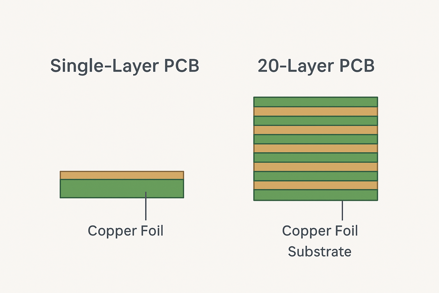
The stackup drawing shows the layers in order, with the copper weight and the dielectric thickness of each. It is drawn from the centre outwards, and the total has to add up to the finished thickness with its tolerance.
The material for each dielectric should be named, at least by the resin system and the glass style, because two materials with the same thickness have different electrical and mechanical properties.
The impedance targets belong on the stackup drawing, with the trace width and the spacing for each controlled line. A shop that is asked to control impedance without those numbers will use its own default geometry.
The stackup guide shows the conventions, and the drawing should be a separate file rather than a note on a copper layer.
Fabrication Notes and Tolerances
The notes should list the surface finish, the mask colour and type, the silkscreen colour and the board thickness with its tolerance. Those items are the ones that the shop would otherwise choose.
The tolerances that matter to the design should be quoted rather than left to the default. The outline tolerance, the hole tolerance, the impedance tolerance and the flatness all fall into this category.
Any feature that requires a special process, such as a plated edge, a counterbore, a press fit hole or a via in pad, has to be described in the notes with the requirement rather than only shown in the artwork.
A note that contradicts the artwork is worse than no note at all, because the shop has to decide which one to follow. The rule is that the artwork defines the geometry and the notes define everything that cannot be drawn, and the two should never overlap.
The notes are also where the acceptance class is recorded, since a board that is inspected to a different class may be accepted or rejected on the same physical result.

IPC Class and Acceptance
The acceptance standard defines what is acceptable and what is a defect, and it is usually quoted by class. Class two is the general industrial default, while class three is used for a product where continuity is critical.
The class affects the price, because a class three board needs tighter inspection and a higher reject rate. Choosing a class that the product does not need is a cost with no benefit.
The class is a property of the product rather than of the board, so it should be decided with the customer and the reliability engineer. A medical or an automotive product usually needs the higher class, while a consumer product rarely does.
The class also affects the design, because the annular ring, the hole breakout and the copper spacing have limits that differ between classes. The limits are in the standard and they should be applied during the layout.
The acceptance criteria should be quoted in the package, so that a disagreement at the end of production can be settled against a document rather than an opinion. The quality judgement depends on it.
Practical Rules
Send one archive with a documented file list, and read the artwork back in a viewer before it is sent.
Include the stackup drawing and the fabrication notes as separate files rather than as notes on a copper layer.
State the tolerance and the acceptance class, and name every special process that the board needs.
Keep the package with the design revision, so that a reorder is built from the same data as the first order.
FAQ
What files does a fabricator need? The copper, mask and silkscreen layers, the drill files, the outline, the stackup drawing and the fabrication notes with the finish and the acceptance class.
Why does the stackup need its own drawing? Because the material and the dielectric thickness are not visible in the artwork, and the shop needs them to buy material and to control the press.
Does the acceptance class change the price? It does, because a higher class needs more inspection and has a lower yield. The class should match what the product actually requires.