



Why Design for Manufacturability Decides PCB Cost and Yield
A PCB can pass every simulation and still be awkward to manufacture. The board may fit the enclosure, route every signal and satisfy the electrical design, yet a combination of small pads, tight spacing, tall components and inaccessible test points can create scrap on the line. Design for manufacturability, usually shortened to DFM, is the work of finding those conflicts while they are still drawings. It connects the designer’s intent with the real capabilities of the fabricator and the assembly house.
That connection matters because a PCB is produced in two very different environments. Fabrication turns the design into a bare board through imaging, drilling, plating, etching, soldermask and surface finish. Assembly then prints solder paste, places components, reflows the board, adds through-hole parts where required, cleans it and tests it. A choice that looks harmless in one stage can become a constraint in the other. DFM gives those constraints a place in the design review instead of leaving them to be discovered after tooling has been ordered.
Start With the Fabrication Stack
The fabrication review begins with the physical board, not with the schematic. Layer count, dielectric thickness, copper weight, drill sizes and the finished surface all influence what the factory can make reliably. The smallest trace and space on the design should be compared with the fabricator’s proven capability, not with a theoretical minimum. The same applies to annular rings, soldermask webs, via aspect ratio and the method used to fill or tent vias.
Copper distribution deserves early attention as well. Large isolated areas, uneven plating and abrupt changes in copper density can make etching and lamination less predictable. A balanced stack helps the board stay flat through reflow and gives the assembly process a more uniform thermal response. When impedance control is required, the stack-up and trace geometry should be agreed before the layout is frozen, because changing them later may force a new set of artwork and a new qualification cycle.
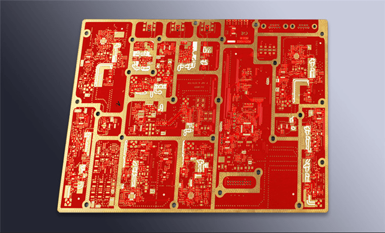
Panel design is part of the same decision. Small boards need rails, spacing and breakout features that allow handling without damage. Fiducials, tooling holes and the distance from the board edge should be planned with the assembly equipment in mind. A board can meet every electrical rule and still be expensive to panel if its outline, copper balance or tooling features force extra handling.
Assembly Rules Are Layout Rules
The assembly review looks at how the finished board will be handled by machines and people. Component courtyards need enough room for the placement nozzle, the feeder path and the rework tool. Parts should be oriented so that polarised devices are easy to verify and so that fine-pitch leads receive paste evenly. Tall components can block the nozzle or create a shadow during reflow, while heavy copper planes can pull heat away from small joints and make the profile uneven across the panel.
Pad geometry is another practical constraint. A footprint that is electrically correct may release too little paste, allow the part to shift during reflow or leave too little room for a reliable solder fillet. Solder mask clearance, stencil aperture design and the relation between adjacent pads all affect bridging and tombstoning. These details are difficult to correct after the stencil and the assembly program have been released, which is why the footprint library should be reviewed against the actual process rather than copied without verification.
Fiducials, test points and board-edge clearance belong in the same conversation. Fiducials should be visible to the placement camera and free of mask or nearby copper that could confuse recognition. Test points should remain accessible after assembly and coating, and connectors placed at the edge must not interfere with conveyor support. If the product uses mixed technology, the through-hole and selective-solder steps must be planned before the SMT layout is finalised, because the sequence determines which side is populated first and which areas need protection.

The Cost Curve Moves Early
Most of the cost of a PCB is fixed by decisions made before the first panel is produced. A footprint change during layout may take minutes. The same change after a stencil, assembly program and inspection recipe have been created can consume engineering time, stop a line and delay a launch. DFM is therefore not only a technical exercise; it is a way to protect schedule and cash flow.
The visible quotation is also an incomplete measure of cost. A low board price can be offset by poor first-pass yield, repeated rework, extra inspection or a batch that must be sorted by hand. A design that uses standard processes where possible, reserves advanced features for the places that need them and gives the factory clear acceptance criteria is usually cheaper over the life of the product than a design that merely looks efficient on paper. The aim is not to remove every difficult feature. It is to make each difficult feature deliberate, understood and supported by the process.
What a Useful DFM Review Produces
A good review is more than a list of generic warnings. Each finding should identify the location, explain the manufacturing consequence and offer a practical choice. Some items must be corrected before tooling. Others can be accepted with a defined process control. A third group may be recorded as a future improvement. Separating those categories prevents a team from treating every comment as equally urgent and helps the project make decisions quickly.
The review should also have an owner and a close-out record. The designer needs to know which files were changed, the fabricator needs the final stack-up and drill data, and the assembler needs the released BOM, placement data and assembly drawing. When one partner suggests a change, the others should have a chance to check the effect. A wider annular ring may help drilling but reduce the space available for routing; a larger paste aperture may improve joint volume but increase bridging risk. DFM works best when these trade-offs are visible to everyone.
Release the Correct Data
Many production problems begin with a documentation mismatch rather than a difficult circuit. The Gerber layers, drill file, stack-up drawing and fabrication notes must describe the same board. The BOM, centroid file, polarity markings and assembly drawing must describe the same build. Footprint names should match the approved component, and the paste and soldermask layers should be checked before the package is sent. Units, board revision and variant options should be stated explicitly.
Version control is equally important. A supplier should not have to guess which file is current or which change note replaces an earlier instruction. Clear release notes, a single point of contact and a written response to open questions reduce the chance that a small correction is applied to one document but missed in another. For prototypes, the same discipline pays off: a clean data package makes the pilot build easier to compare with the eventual production release.
Common Problems That Recur
Some DFM issues appear across many products because they are easy to overlook in CAD. Pads may be too small for consistent paste release. Solder mask webs may be narrower than the fabricator can register reliably. Vias placed in thermal pads may need filling before assembly. Components may sit too close to a connector, a board edge or a tall part. Fiducials may be covered, test points may be buried, or copper may be distributed so unevenly that the board warps during reflow.
None of these problems necessarily requires a complete redesign. The point is to find them early enough to choose the least expensive response. A footprint can be corrected, a fiducial moved, a test point exposed or a panel rail adjusted while the design is still flexible. Waiting until the first batch arrives turns a small layout correction into a production investigation.
Choose a Partner That Reviews Before Building
The strongest manufacturing partner is not the one that accepts every file without comment. It is the one that can explain which features are routine, which need special control and which should be changed before release. That conversation should cover both bare-board fabrication and PCB assembly, including mixed technology PCB assembly when the product uses both surface-mount and through-hole parts.
Ask for a DFM response with specific references to the files, a clear list of assumptions and a path for resolving disagreements. Confirm how changes are controlled, how materials are qualified and how inspection results are recorded. A factory that already works with turnkey PCB assembly should be able to connect fabrication, component sourcing, placement and test without passing responsibility from one department to another.
Test coverage should be part of the same plan. A board that is easy to assemble but impossible to probe may still fail in the field. PCBA testing needs accessible test points, sensible fixtures and a definition of what constitutes a pass. The supporting quality management system should make those results traceable, so a process change can be linked to the batch it affected and a corrective action can be verified.
A Practical Release Checklist
- Confirm the stack-up, copper weight, drill sizes, annular rings, soldermask clearance and surface finish against the fabricator’s capability.
- Check copper balance, panel rails, tooling holes and fiducials before the fabrication package is released.
- Review footprints, courtyards, placement orientation, paste apertures and thermal relief with the assembly process in mind.
- Keep test points, connectors and tall parts clear of nozzles, conveyor support and rework access.
- Match the BOM, centroid data, polarity marks, assembly drawing and revision notes to the same build.
- Record every accepted risk, assign an owner and confirm that the corrected files are the ones released to production.
DFM pays back through fewer surprises, not through a promise that every board will be perfect. It gives the design team a realistic picture of yield, cost and schedule while changes are still inexpensive. That is why the review belongs at the start of the project, alongside the schematic and layout, rather than at the end as a final approval step.