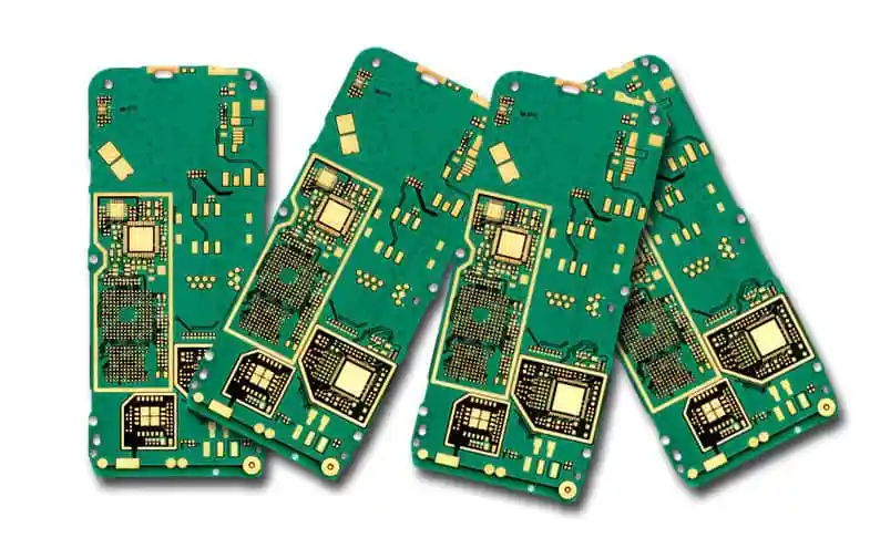
PCB Design Mistakes: The Errors That Reach Production
Most of the errors that stop a board from being built are not electrical. They are documentation and geometry mistakes that pass a design rule check because no rule covers them, and they surface when the fabrication data is processed or when the assembly line tries to place a part. The list below covers the ones that appear most often, grouped by where they cause damage.
Silkscreen and Marking Errors
A reference designator placed over a pad interferes with the assembly process and with in circuit testing, because the probe has to land on solder rather than on ink. It is a placement mistake rather than a layout mistake, and it is invisible in a schematic review.
Text size causes the opposite problem. Text that is too small cannot be printed legibly, and the result is a legend that no one can read; text that is too large produces a silkscreen overlap with the neighbouring designators, which makes the same information unusable in a different way. Both are solved by defining a text size and a clearance for the board and applying it throughout, and by reviewing the silkscreen layer as its own deliverable rather than as an automatic by product of the layout.
Layer Discipline
Drawing on whatever layer happens to be active is convenient while working and destructive afterwards. A connection drawn on a mechanical layer does not appear in the copper data and produces an open circuit; a notation drawn on a copper layer is etched into the board and can produce a short. The Gerber output then either contains a feature that should not exist or omits one that should.
The related error is the accidental extra layer: a four layer design that contains routing on a fifth, unused layer, which is a common result of copying a design or of moving a block between projects. A layer usage report before the data is released catches both, and the report belongs with the rest of the design review.
Convention matters as well. Keeping the component side on the top layer and the solder side on the bottom is an agreement rather than a physical law, but inverting them without saying so produces a board that can be assembled only by someone who has been told what was intended, and assembly documentation is not the place to explain it.

Pad and Hole Problems
Pad overlap is normally a mistake rather than a design. Two pads sharing the same location mean two holes at the same point, which the drill will attempt to drill twice, damaging the drill and the wall. The correct approach for a shared connection is a single pad or a deliberate slot, not two coincident pads.
Overlapping holes are worse in a multilayer board when one of them is a thermal relief and the other a solid connection, because the resulting artwork shows only one of the two patterns and the other is silently lost. The result is a board that is scrapped by the board shop or, worse, one that passes and behaves unpredictably.
Single sided pads deserve their own convention. A pad that is not intended to be drilled should either have no hole at all or be marked so that the drill data does not contain a coordinate for it. If a diameter is present, the drilling step will act on it, producing an unintended hole.
A pad drawn as a filled region is another case where the design tool is satisfied and the process is not. A region does not generate solder mask data in the way a pad does, so the area may be covered by mask and the component cannot be soldered to it. Using the pad object for pads, and reserving regions for copper that has no component, avoids the problem.
Power and Ground Patterns
A thermal relief pattern is a negative in the artwork, which means the drawn shape represents the isolation rather than the connection. Designers who treat the drawn shape as copper produce a plane with the opposite connectivity to the one intended. The practical consequence is a region of the plane that is isolated from the rest, or a plane split that shorts two supplies together.
When several supplies or several ground nets share a layer, the isolation lines between them have to be complete. A single gap in a boundary line connects two nets that were meant to be separate, and the fault appears only after the assemblies fail test. Checking the boundaries as a closed contour rather than as a set of drawn segments is the reliable method.
Geometry That Is Legal but Not Buildable
Fine pitch surface mount pads that are shorter than they need to be will still accept the component, but they leave no room for the test probes, so the in circuit test coverage quietly falls. The pads should be dimensioned with the test access in mind, not only with the placement.
A large copper mesh drawn with very fine gaps is a manufacturing problem. After imaging and development, thin residues of film remain attached to the board between the narrow gaps, and they produce broken traces. The threshold is a property of the imaging process rather than a preference. The spacing threshold in the process specification exists for this reason.
Copper placed too close to the board outline is a separate risk: when the profile is routed, the bit can reach the copper and lift it, taking the solder mask with it. The copper to edge clearance should be treated as a design rule with a defined value rather than left to the outline operation, and the value should come from the fabrication capability.
Slots and routed openings have a similar constraint. A slot that is too narrow in relation to its length cannot be routed reliably, and the ratio between them should follow the process capability. A slot that is too narrow will break the tooling and raise the cost of the board without any benefit to the design.
Even Copper Distribution
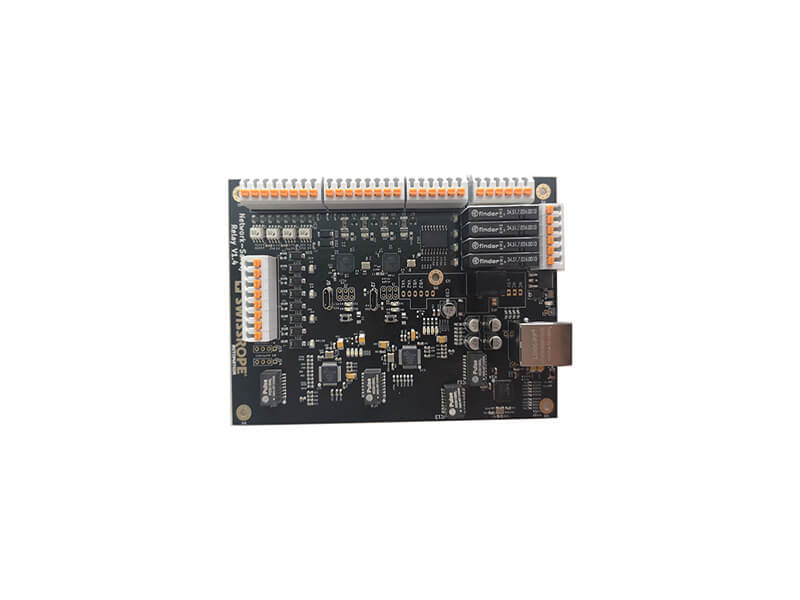
Copper that is concentrated in one area and absent in another creates two problems. During lamination the resin has more volume to fill where there is little copper, which can lead to starvation, and the etching process behaves differently across areas of different density, which affects the final trace width. Designing with a reasonably even copper distribution is one of the cheapest ways to make a board easier to build.
FAQ
Why did the design rule check pass if the board is wrong? The check validates the rules it has. Layer misuse, misregistration of text and process limits are not usually covered by electrical checks.
What is the most common of these mistakes? Silkscreen over pads and drawing on the wrong layer, because both are easy to do and neither produces an error during the layout.
How can the list be checked quickly? Run a layer usage report, review the silkscreen layer as a drawing, verify the mask and drill data against the pads, and confirm the outline clearance against the fabrication capability.
Do these matter on a simple board? Yes. Low layer count designs are where the outline clearance and the slot ratio constraints are most often ignored.
Summary
PCB design mistakes cluster in four places: markings that cover pads or overlap each other, layers used inconsistently, pads and holes that contradict each other, and geometry that the fabrication process cannot reproduce. Each is checkable before the data is released, and each is far cheaper to correct in the editor than in a production line.