PCB Design Review/PCBA Design Review Checklist: DFM and DFA Guide
Why Is PCB/PCBA Design Review Important?
A successful electronic product starts with good design practices. However, even a technically correct schematic and PCB layout can create manufacturing problems if the design is not reviewed from a production perspective.
Before a PCB enters fabrication or a PCBA enters SMT or through-hole assembly, engineers should verify whether the design can be manufactured and assembled reliably. Common issues include:
- BOM components that do not match PCB footprints
- Incorrect or undersized solder pads
- Insufficient spacing between components
- Components positioned too close to the board edge
- Incorrect pin counts or package definitions
- Silkscreen overlapping pads
- Missing or incorrectly positioned fiducial marks
- Manufacturing files that do not match the latest design revision
These problems may not be obvious during schematic or layout design. They can instead appear during PCB fabrication or assembly, resulting in production delays, rework, component replacement, or even a new PCB revision.
A systematic PCB Design Review helps identify these risks before they reach production.
DFM vs. DFA: What Is the Difference?
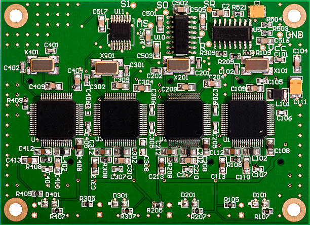
Two important concepts in PCB/PCBA review are DFM and DFA.
What Is PCB DFM Analysis?
PCB DFM Analysis stands for Design for Manufacturing. It evaluates whether a PCB design can be manufactured efficiently and consistently using the selected fabrication process.
Typical DFM checks include:
- Trace width and spacing
- Copper-to-edge clearance
- Hole and via dimensions
- Annular rings
- Layer stackup
- Solder mask openings
- Silkscreen clearance
- Board outline
- Panelization requirements
- Manufacturing tolerances
The goal is to identify design features that may increase manufacturing difficulty, reduce yield, or require additional processing.
For more information on the fabrication side, see GOPCBA PCB Manufacturing.
What Is PCBA DFA Analysis?
PCBA DFA Analysis stands for Design for Assembly. It evaluates whether a PCB can be assembled efficiently and reliably using SMT, through-hole, or mixed-technology processes.
DFA checks may include:
- Component-to-component spacing
- Component-to-board-edge clearance
- Footprint and pad compatibility
- Pin and pad configuration
- Component orientation
- Silkscreen placement
- Fiducial marks
- Soldering access
- Assembly constraints
The objective is to reduce assembly difficulties, improve production efficiency, and minimize defects.
For complex products, DFA should be considered together with the actual assembly process. GOPCBA PCB Assembly Services can be used as a reference when evaluating production requirements.
PCB/PCBA Design Review Checklist
A practical review should cover both the PCB itself and the relationship between the PCB, BOM, and component footprints.
1. Component Spacing
Check the clearance between adjacent components, pads, and other structures.
Insufficient spacing can cause:
- Solder bridging
- Component interference
- Placement-machine limitations
- Inspection difficulties
- Rework problems
Spacing requirements should be evaluated according to component package, assembly process, component height, and manufacturing capability.
2. Component-to-Board-Edge Clearance
Components positioned too close to the board edge may interfere with:
- PCB routing
- Depanelization
- SMT tooling
- Fixtures
- Mechanical assembly
Sensitive or tall components may require additional clearance beyond the minimum fabrication requirement.
3. Silkscreen and Reference Designators
Reference designators and other silkscreen markings should remain readable and should not overlap solder pads or critical component areas.
Incorrect or misplaced reference designators can also increase the risk of component placement errors during assembly.
4. Pin and Pad Matching
The number and arrangement of component pins must match the corresponding PCB footprint.
A mismatch between the BOM component and PCB footprint can result in components that cannot be properly soldered or electrically connected.
This is especially important for connectors, ICs, fine-pitch packages, and through-hole components.
5. SMT Pad Design
Solder pad dimensions should be appropriate for the selected component package and assembly process.
Incorrect pad dimensions can contribute to:
- Insufficient solder joints
- Solder bridging
- Tombstoning
- Poor component alignment
- Open solder joints
Pad geometry should therefore be checked against the component manufacturer’s recommended land pattern whenever possible.
6. Through-Hole Pad and Hole Design
For through-hole components, both hole diameter and pad geometry need to match the component leads and PCB fabrication capability.
An undersized hole can prevent component insertion, while excessive clearance may reduce soldering reliability.
7. Fiducial Marks
Fiducial marks provide optical reference points for automated component placement and inspection equipment.
Engineers should verify:
- Fiducial quantity
- Location
- Size
- Clearance around the fiducial
- Visibility to the assembly equipment
Incorrect fiducial placement can affect automated placement accuracy.
8. Pad Connectivity
Every required pad should have the intended electrical connection.
Unconnected pads or incorrect copper connections can result in:
- Open circuits
- Incorrect signal paths
- Assembly defects
- Functional failures
A connectivity check should therefore be included before manufacturing files are released.
BOM and PCB Footprint Verification
The BOM and PCB layout should be reviewed together rather than independently.
Important items to verify include:
| Check Item | What to Verify |
|---|---|
| Part number | Matches the intended component |
| Package | Matches the PCB footprint |
| Pin count | Matches the footprint |
| Pin pitch | Matches the pad layout |
| Component orientation | Correct polarity and orientation |
| Reference designator | Matches BOM and PCB |
| Manufacturer information | Correct approved component |
| Alternate parts | Compatible with the existing footprint |
This type of cross-check is particularly important when a design contains many similar components.
A mismatch between the BOM and PCB footprint may remain unnoticed until procurement or assembly, making early verification much more cost-effective.
PCB Manufacturing File Review
Before releasing production data, engineers should also check whether all manufacturing files belong to the same design revision.
Depending on the project, the production package may include:
- Gerber files
- Drill files
- ODB++ data
- Pick-and-place files
- BOM
- Assembly drawings
- Fabrication drawings
- Stackup information
- Test requirements
The PCB manufacturer and assembly provider should work from a consistent and clearly identified revision.
For projects involving both fabrication and assembly, GOPCBA PCB Design & Layout can help align design requirements with downstream manufacturing considerations.
Useful PCB Design Checks Before Production
A comprehensive review can also include several additional checks.
Electrical Connectivity
Verify that all intended nets are correctly connected and that unintended shorts are not present.
Copper and Clearance
Check trace width, copper spacing, copper-to-edge clearance, and other design-rule requirements against the selected fabrication process.
Board Outline
Confirm that the PCB outline matches the mechanical design and that mounting holes, cutouts, slots, and other mechanical features are correctly positioned.
Panelization
If multiple PCBs will be assembled as a panel, verify the panel arrangement, tooling features, fiducials, board orientation, and depanelization method.
Component Orientation
Standardize component orientation where practical. Consistent orientation can simplify automated assembly and visual inspection.
Thermal Considerations
High-power components, thermal pads, copper areas, and heat dissipation structures should be reviewed to ensure the PCB can meet the expected thermal requirements.
DFM and DFA Should Be Performed Before Production
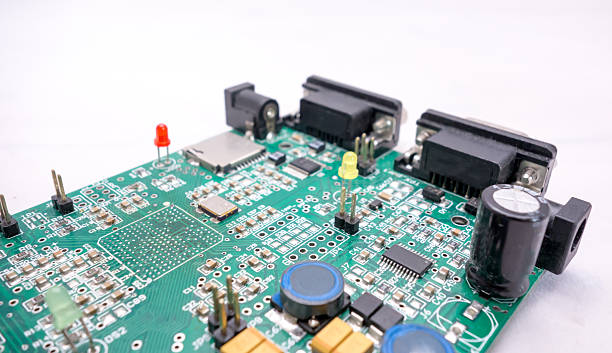
DFM and DFA are not simply final inspection steps. They should be integrated into the design process as early as possible.
A typical workflow is:
Schematic → PCB Layout → DFM Review → DFA Review → BOM/Footprint Verification → Manufacturing Data Review → PCB Fabrication → PCB Assembly → Testing
Early design review allows engineers to identify problems while changes are still relatively inexpensive.
Once a PCB has entered fabrication or assembly, correcting the same problem may require:
- PCB rework
- Component replacement
- Assembly rework
- Production delays
- New PCB fabrication
- Additional engineering costs
For prototype projects, an early review is especially valuable because design problems can be corrected before moving to larger production volumes. GOPCBA Prototype PCB Assembly provides a suitable production path for prototype-stage validation.
PCB/PCBA Design Review Checklist
Before releasing a design to production, engineers can use the following quick checklist:
PCB Fabrication
- Board dimensions and outline are correct
- Layer count and stackup are correct
- Trace width and spacing meet fabrication requirements
- Hole and via dimensions are appropriate
- Copper-to-edge clearance is acceptable
- Solder mask openings are correct
- Silkscreen does not overlap critical areas
- Mounting holes and slots are correctly positioned
PCB Assembly
- Component spacing is sufficient
- Component-to-edge clearance is sufficient
- Footprints match component packages
- Pin counts and pad layouts are correct
- SMT pad dimensions are appropriate
- Through-hole dimensions match component leads
- Fiducial marks are correctly positioned
- Component orientation is correct
BOM and Manufacturing Data
- BOM matches the latest PCB revision
- Reference designators are consistent
- Component part numbers are correct
- Pick-and-place data matches the PCB
- Gerber/ODB++ data matches the approved revision
- Assembly drawings are up to date
- Manufacturing notes are complete
Conclusion
A good PCB design is not necessarily a production-ready PCB design. Before fabrication and assembly, engineers need to evaluate both manufacturability and assembly requirements.
PCB DFM Analysis focuses on whether the board can be fabricated efficiently and consistently, while PCBA DFA Analysis focuses on whether components can be assembled reliably and efficiently.
By combining DFM, DFA, BOM verification, footprint checking, electrical connectivity analysis, and manufacturing-data review, engineers can identify potential production risks before they become expensive manufacturing problems.
A structured PCB Design Review is therefore an important step between PCB layout and production. It helps reduce redesigns, improve manufacturing yield, shorten development cycles, and create a more reliable transition from engineering design to finished PCBA.
For production projects requiring PCB fabrication, component sourcing, assembly, and testing, integrating these checks into the entire manufacturing workflow can provide greater consistency from prototype to volume production.