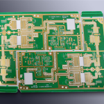
Etch Compensation on PCB: 6 Rules That Hold Trace Width
Etch compensation is the deliberate widening of the artwork so that the finished trace reaches its designed width after etching. The etchant removes metal sideways as well as downwards, and if the artwork were drawn at the target width, the finished conductor would come out narrower and, on a controlled impedance layer, electrically different from the design.
The amount added is not a fixed number. It depends on copper thickness, etchant chemistry, line width, the pattern density around the trace and the process the shop runs, which is why compensation values belong to a specific fabrication line rather than to a general rule. A shop that has measured its own process can hold fine lines that another shop would have to widen, and the difference shows up in the coupon data rather than in the drawing.
<img src="https://www.gopcba.com/wp-content/uploads/2026/08/pcb-assembly-image.jpg" alt="Cross section of a PCB trace showing the sidewall left after etch compensation” />
Why Artwork Is Wider Than the Finished Trace
Etching is isotropic at the surface. The etchant attacks the copper in every direction it can reach, so while the top surface is dissolving downwards, the sides are also being undercut beneath the resist. The finished conductor therefore has a trapezoidal cross section rather than a rectangular one.
Compensation pushes the artwork outward along both edges to allow for that loss. The designer specifies the finished width and the fabricator adds the allowance, which is why the same design produced at two shops can have different artwork and the same measured result, provided both control their processes.
What Happens at the Etch Edge
The edge of a trace is where the resist, the copper and the chemistry meet, and it is the part of the profile that varies most. Fresh etchant reaching the edge cuts quickly, while exhausted etchant trapped beside a narrow gap cuts slowly, so a trace beside a wide copper area etches differently from an isolated one. Spray pressure and nozzle condition decide how well fresh chemistry reaches that trapped volume, which is why etch uniformity is a machine condition as much as a chemical one.
That local variation is the reason pattern density matters. A dense array of fine lines etches more slowly than an open area on the same panel, and the shop compensates with the process rather than with the artwork for the difference. The measurable result is a trace width distribution across the panel, not a single value.
The Etch Factor and How It Is Measured
The etch factor is the ratio of the sideways undercut to the depth of copper removed. A high factor means the etchant cuts mostly downwards and leaves steep sidewalls, while a low factor means more lateral attack and a shallower sidewall angle.
The factor is not a constant. It depends on chemistry, spray or immersion conditions, temperature, copper thickness and, most strongly, on how wide the feature is. Shops measure it by etching coupons with a range of line widths and measuring the resulting profile on a section or with an optical system.
Copper Thickness and Compensation
Thicker copper must be etched for longer, and longer etching means more sideways attack. A two ounce layer therefore needs a larger compensation than a one ounce layer for the same finished width, and the difference grows quickly as the target width falls.
This is the practical limit on fine lines in heavy copper. The copper weight and the minimum line width have to be chosen together, because at some combination the compensating artwork becomes so wide that two adjacent lines cannot be supported on the resist. Where a design needs both heavy copper and fine lines, the usual answer is a different process route rather than a tighter etch.
Compensation for Impedance Controlled Lines
On an impedance controlled layer the width and the thickness are both inputs to the calculation, so compensation affects the electrical result directly. The trapezoidal profile also has to be modelled, since the effective cross section of a trapezoid differs from the rectangle the design assumed.
This is why impedance tolerance is quoted with the stack-up and the finish, and why a coupon is built into the panel. A change to compensation, to plating thickness or to the laminate shifts the measured impedance even when the artwork and the stack-up drawing are unchanged.
Compensation, Registration and Annular Ring
Compensation interacts with layer to layer registration. A pad that is widened for etching also has to be positioned accurately relative to the drilled hole, and both errors consume the same annular ring. If registration drifts while compensation stays constant, the ring shrinks on one side of the hole before it shrinks on the other.
Design rules usually express this as a minimum annular ring that has to survive the worst case combination of drill tolerance, registration and etch loss. That budget is what the compensation value has to fit inside, and it is normally reviewed by the fabricator before a design is released.
Etchant Chemistry and Its Effect
Different etchants produce different profiles. Acidic copper chloride systems are common for inner layers, while alkaline ammonia chemistry is used where the resist requires it, and the two behave differently for the same copper thickness and line width.
Bath control matters as much as the chemistry choice. Copper concentration, acidity, oxidiser level and temperature all change the etch rate, and a bath that is running slow will be pushed with a longer dwell or a higher temperature, which increases lateral attack and changes the finished width without any artwork change. Logging etch rate against the coupon measurement is what links the bath condition to the geometry the customer receives.
Verifying Compensation on the Finished Board
Verification uses a coupon on the panel that carries the same line widths and the same spacing as the product. The finished width is measured optically or on a section, and the results are compared with the drawing to establish whether the compensation in use is still correct.
The measurement should cover the narrowest line, a mid-range line and an isolated line, because the compensation error is largest at the extremes. A shop that checks only a convenient wide trace will find the process in specification while the fine lines on the same panel are out of tolerance.
Where Compensation Goes Wrong
The most common error is using a compensation value from another shop or another product family. Values are specific to a line, and importing them produces a systematic width error that appears on every board until someone measures the coupon properly.
The second is a change in an upstream process that nobody connects to the etch. A new plating thickness, a different laminate or a revised dry film resist all change the starting condition, and the etch result moves with them. Because the finished board still looks correct, the cause is rarely found without coupon data.
FAQ
Is etch compensation the same for every trace on a panel? No. Width, spacing and local pattern density all affect the amount of undercut, so a shop applies a compensation that reflects the feature size and the surrounding copper rather than one value for the whole layer.
How is the correct value established? By etching a test pattern with a range of widths on production material and measuring the result. The value that brings the finished widths inside tolerance across the range is the one the shop adopts for that process.
Does compensation change impedance? It changes the finished geometry, which is what the impedance calculation depends on. The artwork is adjusted so the finished trace matches the design, so compensation is part of the impedance control chain rather than a separate cosmetic step.