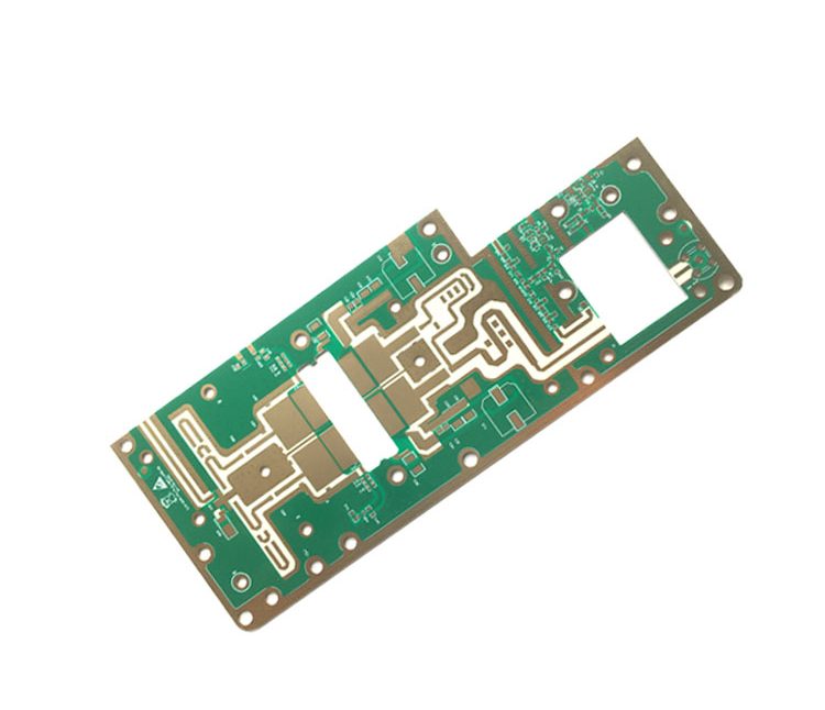
Screen Printing and Stencil Making for PCB Production
Printing is used on a circuit board for two different purposes: the legend and solder mask applied by the fabricator, and the solder paste applied by the assembly house. Both rely on a patterned tool, and in both cases the quality of that tool determines how faithfully the pattern is reproduced.
Where Printing Is Used
Screen printing applies ink through a mesh that carries a photosensitive emulsion patterned with the image. It is used for solder mask and legend because both are printed rather than imaged directly, and because the process is economical at production volumes.
Solder paste printing uses a metal stencil rather than a mesh. The paste is a thixotropic mixture of alloy powder and flux, and the aperture, the stencil thickness and the release properties determine the volume deposited on each pad, as described in the general rules for solder mask and paste behaviour.
Direct and Indirect Stencil Methods
The direct method coats the tensioned mesh itself with emulsion, exposes it through a film and develops the image in place. It is the simpler route and produces a durable screen, but each screen has to be prepared individually.
The indirect method forms the image on a separate film that is then transferred to the mesh, which gives better dimensional accuracy because the film is imaged flat. Combinations of the two are also used where the accuracy of the film matters and the durability of the direct coating is wanted.

Mesh and Emulsion
The mesh count sets the resolution limit. A fine mesh reproduces small features but passes less ink, while a coarse mesh deposits more ink and cannot hold fine detail. The choice follows the smallest feature in the image and the thickness required.
The emulsion acts as a photoresist: it is the photosensitive layer that carries the pattern. A diazo based emulsion is common for its durability and exposure latitude, and it is prepared by mixing the sensitiser into the base and allowing it to stand before use so that the reaction completes uniformly.
Coating the Screen
Coating is done in two stages. The squeegee side is coated first to fill the openings of the mesh and remove air, and the print side is coated afterwards to build the thickness that controls the ink deposit.
Each pass adds a few microns, so the required thickness is built up by repeating the sequence with drying between passes. Coating the squeegee side too heavily produces uneven exposure and a screen that fails early, while coating the print side too thinly produces a stencil that wears out quickly.
Drying
Drying has to remove the water evenly without hardening the surface before the interior is dry. A temperature around 40 to 45 degrees Celsius for about ten minutes is typical, and a higher temperature causes the surface to skin over while moisture remains beneath it.
Temperature also affects the mesh. Excessive heat changes the tension of the woven fabric, which alters the registration of the printed image and the ink deposit across the screen. Controlling the drying temperature is therefore a dimensional control as much as a chemical one.
Exposure and Its Verification
Exposure polymerises the emulsion where light passes through the clear areas of the film. Too little exposure leaves the coating soft and it washes away during development, while too much hardens the edges and closes fine detail.
The correct energy is established with an exposure calculator: a test pattern with several densities is exposed and developed, the best result is identified, and the exposure time is adjusted by the factor marked against that patch. The procedure is repeated once more to confirm the setting.
Development and Finishing
Development washes away the unexposed emulsion and leaves the pattern. The screen is then dried, any small defects are touched in, and a final exposure hardens the whole coating before the screen is sealed and put into use.
Defects found at this stage are corrected before printing rather than after, which is the point of the inspection step. A pinhole in the emulsion becomes a missing feature on every board printed with that screen.
Metal Stencils for Solder Paste
Solder paste stencils are cut from stainless steel sheet rather than printed, usually by laser, with the walls of the aperture finished to promote clean release. The thickness of the sheet is chosen from the paste volume required and the smallest pitch on the board.
For very small apertures a stepped stencil is used, where the area over fine pitch parts is thinner than the area over connectors. That allows two different paste volumes to be deposited in one print, which is the technique used where through hole parts are reflowed, as described in the through hole soldering process.
Stencil and Aperture Design
The aperture area ratio governs release. A small aperture in a thick stencil has a large wall area relative to its volume, and the paste tends to stay in the hole rather than transferring to the pad, so the ratio should be kept above the accepted minimum.
Aperture shape matters too. A slight rounding of the corners and a small reduction in size relative to the pad reduce bridging and paste spread, and the pad design should provide enough area for the aperture to be defined without encroaching on the mask.
Cleaning and Screen Life
A screen that is cleaned properly lasts through many print cycles. Ink left in the mesh hardens and blocks the openings, and aggressive cleaning damages the emulsion, so both the chemistry and the method matter.
Life is also limited by mechanical wear. The squeegee pressure that forces ink through the mesh also abrades the coating, and a screen that has lost thickness prints a lighter deposit. Tracking the number of prints and inspecting periodically is what prevents a gradual drift in quality.
Quality Checks
Before use, the screen or stencil is inspected for pinholes, blocked openings and damage, and its dimensions are checked against the artwork, particularly where registration to the pad is critical.
Once printing begins, the result is monitored rather than the tool. Deposit weight, print definition and registration on the board tell you what the process is doing, and those measurements catch a worn screen before it produces a batch of defective assemblies.
Registration and Print Parameters
Registration is the alignment between the printed image and the features already on the board. It is set by the tooling holes, the screen frame and the printer, and it is checked on the first article before the batch is run.
Squeegee pressure, speed and the snap-off distance between the screen and the board all affect the result. Too much pressure distorts the mesh and smears the image, while too little leaves ink in the openings, so the parameters are established and then left alone.
From Print to Cure
Printing is followed by a settling period and then a cure. The settling allows the ink to level, which removes the marks of the mesh, and the cure drives off solvent and cross-links the resin into the final film.
The cure profile matters as much as the print. An under-cured mask remains soft and can be damaged during assembly, while over-curing makes it brittle. Both conditions show up later as defects that appear unrelated to the printing step.
FAQ
Why is a metal stencil used for solder paste but a mesh for solder mask? Paste needs a precise volume and a clean release from a thin, dimensionally stable aperture, while mask is an ink that is applied in a controlled thickness through a durable screen.
How is the correct exposure determined? With an exposure calculator that tests several densities in one pass. The best patch indicates the factor by which the trial time should be multiplied.
What causes a pinhole in the printed image? A defect in the emulsion, usually from contamination during coating or from damage during development. It reproduces on every board until the screen is repaired.