PCB Failure Analysis: PCB Design, PCB Manufacturing & Common PCB Failures
Printed circuit boards (PCBs) are the foundation of countless electronic products and systems. From consumer electronics and industrial equipment to automotive systems, medical devices, and communication equipment, PCBs provide the electrical and mechanical platform that allows electronic components to work together.
However, a PCB can experience various types of failures throughout its lifecycle. Manufacturing defects, component problems, electrical overstress, thermal stress, environmental exposure, improper handling, and aging can all affect PCB reliability and performance.
Regular inspection and systematic PCB Failure Analysis can help identify early warning signs before they develop into serious functional problems. By understanding common PCB failure modes and their causes, engineers can improve PCB Design, manufacturing quality, testing procedures, and long-term product reliability.
This article examines eight common PCB failure conditions and provides practical guidance for identifying and preventing them.
What Is PCB Failure Analysis?
PCB Failure Analysis is a systematic process used to identify, investigate, and determine the root cause of a PCB malfunction or physical defect.
Depending on the failure, analysis may involve:
- Visual inspection
- Electrical testing
- Continuity and isolation testing
- Thermal inspection
- Component testing
- Microscopic inspection
- X-ray inspection
- Signal measurement
- Solder joint inspection
- Environmental evaluation
- Design and manufacturing data review
The purpose is not simply to identify that a PCB has failed. A complete failure analysis should determine why the failure occurred, where it originated, and how similar failures can be prevented in future designs or production batches.
1. Physical Damage
Physical damage is one of the most obvious causes of PCB failure. A circuit board can be damaged during manufacturing, assembly, transportation, installation, maintenance, or normal operation.
Common forms of physical PCB damage include:
- Cracked circuit boards
- Broken traces
- Scratches
- Bent boards
- Broken connectors
- Damaged components
- Delamination
- Lifted pads
- Damaged solder joints
- Cracked vias
- Broken mounting holes
Even relatively small mechanical defects can affect electrical continuity or mechanical reliability.
For example, excessive bending can create stress around vias, solder joints, connectors, and component leads. In multilayer PCBs, mechanical stress can also damage internal structures that are difficult to identify through a simple visual inspection.
During PCB Manufacturing and assembly, proper handling procedures should therefore be established to minimize mechanical stress. Operators should also use appropriate fixtures and ESD-safe handling practices when required.
2. Electrical Shorts and Open Circuits
Electrical shorts and open circuits are among the most common PCB failure modes.
An open circuit occurs when an intended electrical path is interrupted. A broken trace, defective via, cracked solder joint, or poor connection can prevent current or signals from reaching the intended destination.
A short circuit, in contrast, creates an unintended low-resistance connection between two electrical nodes.
Shorts can occur because of:
- Solder bridges
- Insufficient PCB spacing
- Copper burrs
- Manufacturing contamination
- Component damage
- Conductive debris
- Incorrect assembly
- Design errors
Depending on the circuit, a short circuit can cause excessive current, overheating, component damage, or power-supply protection to activate.
PCB manufacturers can detect many open and short conditions through electrical testing. Depending on production volume and board complexity, testing may involve flying-probe systems, fixture-based testers, continuity testing, or isolation testing.
A multimeter can also be useful during troubleshooting, particularly for prototypes, repairs, and localized fault investigation.
3. Overheating and Thermal Stress
Electronic components and conductive structures generate heat during operation. A properly designed PCB must provide an appropriate thermal path so that heat can be dissipated within the required operating limits.
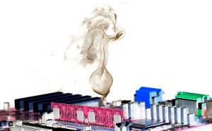
Excessive temperature can result from:
- High current density
- Insufficient copper area
- Poor thermal management
- Inadequate heat sinking
- High-power components
- Poor component placement
- Insufficient airflow
- Excessive ambient temperature
- Incorrect component selection
Long-term thermal stress can accelerate component aging and degrade solder joints, laminates, and other materials.
During PCB Design, engineers should evaluate thermal requirements early in the development process. Depending on the application, thermal design may include:
- Larger copper areas
- Thermal vias
- Heat sinks
- Metal-core PCB structures
- Appropriate component spacing
- Controlled current density
- Improved airflow
- Thermal simulation
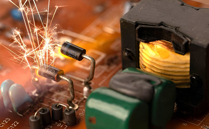
During troubleshooting, engineers should look for signs such as discoloration, burned components, damaged solder joints, abnormal temperature rise, or unusual odors.
Thermal imaging can also help identify localized hot spots that are difficult to detect through visual inspection.
4. Corrosion, Dust, and Moisture
Environmental exposure can gradually degrade PCB performance.
Unlike obvious mechanical damage, environmental damage may develop slowly over months or years. Moisture, dust, corrosive gases, salt contamination, and chemical residues can affect conductive surfaces and insulation properties.
Potential consequences include:
- Copper corrosion
- Oxidation
- Leakage currents
- Reduced insulation resistance
- Dendritic growth
- Connector degradation
- Solder joint deterioration
- Intermittent electrical failures
Environmental risks are particularly important in outdoor, automotive, industrial, marine, and other demanding applications.
PCB protection methods may include:
- Conformal coatings
- Protective enclosures
- Appropriate surface finishes
- Controlled storage conditions
- Proper cleaning
- Moisture management
- Contamination control
During PCB Manufacturing, appropriate cleaning and surface-treatment processes can reduce contamination-related risks. However, the exact protection method should be selected according to the operating environment and product requirements.
5. Signal Loss and Abnormal Output
Not all PCB failures are visible. A board may appear physically normal while producing incorrect signals, unstable outputs, or intermittent operation.
Possible symptoms include:
- Signal loss
- Unexpected voltage levels
- Intermittent operation
- Communication errors
- Incorrect sensor readings
- Abnormal output signals
- System resets
- Complete loss of functionality
Potential causes include:
- Broken or high-resistance connections
- Damaged components
- Poor solder joints
- Incorrect impedance
- Crosstalk
- Excessive electromagnetic interference
- Power integrity problems
- Grounding problems
- Signal-integrity issues
- PCB design errors
For high-speed circuits, signal behavior can be affected by trace geometry, dielectric properties, layer stackup, impedance control, return paths, and routing topology.
Consequently, effective PCB Design should consider signal integrity before physical routing is finalized.
Depending on the application, engineers may use an oscilloscope, multimeter, logic analyzer, spectrum analyzer, TDR, or other diagnostic equipment to locate signal-related failures.
6. Aging and Lifecycle Factors
PCBs are integrated systems containing numerous components and materials, each with its own operating limits and expected service life.
Although the PCB substrate itself may remain physically intact, individual components can degrade over time.
Common aging-related problems include:
- Capacitor degradation
- Solder joint fatigue
- Connector wear
- Relay degradation
- Thermal cycling damage
- Material aging
- Surface oxidation
- Insulation degradation
The service life of a PCB assembly therefore depends on more than the durability of the bare board.
During PCB Design, engineers should consider component lifecycle, operating temperature, electrical stress, mechanical stress, environmental conditions, and expected product service life.
Component derating can also be used where appropriate to reduce operating stress and improve reliability.
For products expected to remain in service for many years, engineers should also monitor component lifecycle status and plan for potential obsolescence.
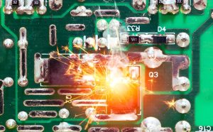
7. Component Failure
A PCB may contain hundreds or thousands of components with different electrical, mechanical, and thermal characteristics. Any individual component can potentially fail and affect the operation of the entire assembly.
Component failures may result from:
- Electrical overstress
- Excessive voltage
- Excessive current
- Thermal stress
- Manufacturing defects
- ESD events
- Mechanical damage
- Incorrect component selection
- Aging
- Poor soldering
- Environmental exposure
Some failed components are easy to identify through visual inspection. For example, a burned resistor or cracked capacitor may be immediately visible.
Other failures are internal and require electrical testing.
A systematic troubleshooting process can include:
- Confirm the failure symptom.
- Inspect the PCB visually.
- Check the power supply.
- Measure key voltages and resistances.
- Test suspected components.
- Compare measurements with the design requirements.
- Replace or repair the defective component where appropriate.
- Retest the complete assembly.
Selecting reliable components during PCB Design and maintaining appropriate sourcing controls during production can reduce component-related failures.
8. Improper Storage and Handling
Storage and handling are sometimes overlooked when investigating PCB reliability.
Even a well-designed and correctly manufactured PCB can be damaged if it is improperly stored, transported, or handled.
Potential risks include:
- Electrostatic discharge
- Moisture absorption
- Mechanical impact
- Excessive bending
- Contamination
- Oxidation
- Incorrect temperature or humidity
- Improper packaging
ESD is particularly important for sensitive electronic components. Personnel handling PCBs should follow appropriate ESD-control procedures when required by the product and manufacturing process.
PCB storage conditions should also be controlled according to the requirements of the board materials, components, and applicable manufacturing procedures.
Moisture-sensitive components may require additional controls, such as moisture-barrier packaging and humidity monitoring.
During transportation, protective packaging should prevent mechanical shock, vibration, contamination, and moisture exposure.
PCB Failure Analysis Methods
Identifying the failure mode is only the first stage. Engineers should use a structured diagnostic process to determine the root cause.
Visual Inspection
Visual inspection is usually the first step because it is fast and non-destructive.
Inspect for:
- Burn marks
- Cracks
- Corrosion
- Broken components
- Lifted pads
- Solder bridges
- Poor solder joints
- Contamination
- Delamination
- Discoloration
Microscopes or digital inspection systems can be used for small components and fine-pitch connections.
Electrical Testing
Electrical testing can identify open circuits, short circuits, abnormal resistance, and other electrical problems.
Common methods include:
- Continuity testing
- Isolation testing
- Resistance measurement
- Voltage measurement
- Insulation resistance testing
- In-circuit testing (ICT)
- Functional testing
Thermal Inspection
Thermal inspection is useful when the failure is related to excessive current, short circuits, or abnormal power dissipation.
Infrared cameras can help identify unexpected hot spots and thermal gradients.
X-Ray Inspection
X-ray inspection is useful for defects that cannot be seen from the PCB surface.
It can help inspect:
- Hidden solder joints
- BGA connections
- Voids
- Internal connections
- Certain multilayer structures
Design and Manufacturing Data Review
A failure may originate from either design or manufacturing.
Therefore, engineers should review:
- Schematic
- PCB layout
- Stackup
- Gerber files
- Drill files
- BOM
- Assembly files
- Manufacturing records
- Test results
- Component specifications
Comparing these records can help determine whether the problem originated during design, fabrication, assembly, or field operation.
How to Prevent Common PCB Failures
Preventing PCB failures is generally more efficient than repairing defective products after they enter the field.
During PCB Design
Engineers should consider:
- Adequate trace width and spacing
- Controlled impedance where required
- Proper power distribution
- Effective grounding
- Thermal management
- Component derating
- Appropriate creepage and clearance
- Manufacturability
- Mechanical constraints
- Environmental conditions
- Component lifecycle
Design-for-Manufacturing (DFM) and Design-for-Testing (DFT) practices can also help identify potential problems before production.
During PCB Manufacturing
Manufacturers should maintain process controls for:
- Lamination
- Drilling
- Plating
- Etching
- Solder mask
- Surface finishing
- Electrical testing
- Dimensional inspection
For PCB assembly, additional controls may include solder paste printing, component placement, reflow soldering, AOI, X-ray inspection, and functional testing where required.
During Storage and Operation
Finished PCBs should be protected from:
- Excessive moisture
- Dust
- Corrosive environments
- ESD
- Mechanical shock
- Excessive temperature
- Improper handling
The protection strategy should match the intended application and environmental requirements.
PCB Failure Analysis Checklist
When troubleshooting a defective circuit board, the following checklist can provide a practical starting point:
| Inspection Area | Key Checks |
|---|---|
| Physical condition | Cracks, bending, delamination, broken parts |
| Electrical | Opens, shorts, abnormal resistance and voltage |
| Components | Burned, cracked, incorrect, or failed components |
| Soldering | Bridges, insufficient solder, poor joints |
| Thermal | Hot spots, overheating, discoloration |
| Environment | Moisture, corrosion, dust, contamination |
| Signals | Missing, unstable, or abnormal signals |
| Documentation | Schematic, layout, BOM, Gerber and assembly files |
| Testing | ICT, AOI, X-ray, functional testing where applicable |
| Handling | ESD, storage, transportation, and mechanical damage |
How Kingda Can Help Improve PCB Reliability
Reliable PCB production requires coordination between PCB Design, fabrication, component sourcing, assembly, and testing.
At Kingda, engineering and manufacturing considerations can be integrated throughout the PCB production workflow. Reviewing design data, component information, fabrication requirements, and assembly requirements before production can help identify potential manufacturing risks at an early stage.
A systematic approach to PCB quality can help reduce:
- Manufacturing defects
- Component-related failures
- Assembly problems
- Electrical defects
- Thermal problems
- Material-related risks
- Field failures
For complex or high-reliability applications, PCB failure prevention should begin during the design stage rather than after the finished product fails.
Conclusion
PCB failures can result from many different factors, including physical damage, open and short circuits, overheating, environmental exposure, signal-integrity problems, component aging, component failure, and improper storage or handling.
Because these failure modes have different symptoms and root causes, effective PCB Failure Analysis requires a systematic approach rather than relying on visual inspection alone.
The most effective strategy is to address reliability throughout the entire product lifecycle—from PCB Design and component selection to PCB Manufacturing, assembly, testing, storage, and field operation.
By identifying early warning signs, maintaining appropriate inspection procedures, controlling manufacturing processes, and keeping accurate technical documentation, engineers and manufacturers can reduce the risk of major PCB failures and improve the long-term reliability of electronic products.