PCB Functional Testing: How to Customize a Reliable Test Solution
Printed circuit boards (PCBs) provide the electrical foundation for modern electronic products, and their functional performance directly affects the reliability of the final device. Because different PCBs handle different signal types, power requirements, interfaces, and functional modules, a standardized testing process may not always provide sufficient coverage.
A well-designed PCB functional testing solution should therefore be customized according to the specific application, circuit architecture, performance requirements, and potential failure risks. The objective is not simply to test as many parameters as possible, but to accurately identify critical risks while maintaining testing efficiency and cost control.
From requirement analysis to test execution and optimization, a customized PCB test strategy should establish a complete and traceable process for verifying PCB functionality and reliability.
1. Define Testing Requirements Before Developing the Test Solution
Before creating a PCB testing strategy, engineers should first analyze the PCB’s application environment, functional characteristics, electrical specifications, and potential risks.
This initial analysis provides the foundation for determining which tests are necessary and how each test should be performed.
Map the Application to Functional Requirements
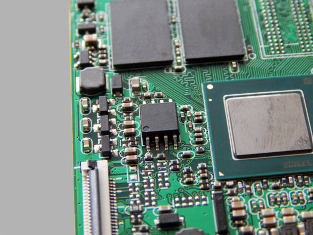
Different applications place different demands on PCB performance.
For example, an IoT device designed for low-power wireless communication may require particular attention to RF signal transmission and low-voltage power circuits. An industrial control PCB used for signal acquisition and control output may require more emphasis on analog signal accuracy, digital response time, and communication interfaces.
For consumer electronics with multiple external interfaces, testing may need to focus on USB, audio, wireless communication, and the interaction between different functional modules.
Mapping application requirements to PCB functions helps eliminate unnecessary tests while ensuring that critical functions receive adequate coverage.
Convert Performance Requirements Into Measurable Standards
The phrase “the PCB works normally” is not sufficient as a professional testing criterion.
Each important requirement should be converted into measurable parameters.
For power stability, the test specification may define the operating voltage range, maximum load current, allowable voltage drop, and voltage ripple.
For high-speed signal transmission, engineers may define data rate, signal delay, impedance, or other relevant electrical parameters.
For interface compatibility, the required protocol versions, communication rates, and acceptable transmission error rates should be clearly specified.
These measurable criteria make test results objective, repeatable, and traceable.
Identify Potential Risks and Set Test Priorities
Test resources should be concentrated on functions with higher potential impact or failure probability.
For example, if a PCB contains high-voltage power circuits close to low-voltage signal circuits, electrical isolation should receive appropriate testing attention.
If several functional modules operate simultaneously, engineers should evaluate whether their operation causes signal interference or functional conflicts.
Similarly, a critical interface used for communication between the PCB and the main system may require a higher test coverage level than a non-critical auxiliary interface.
Risk-based prioritization makes PCB functional testing more efficient while improving the ability to detect important defects.
2. Core PCB Functional Testing Items
A customized PCB test solution should cover the electrical, signal, interface, and functional aspects that are critical to the product.
The exact test combination should be determined according to the PCB design and application requirements.
Electrical Performance Testing
Electrical performance is the foundation of PCB operation. Testing should verify whether power and signal circuits operate within their specified electrical parameters.
Power Circuit Testing
A DC power supply and electronic load can be used to simulate different operating conditions.
Engineers can apply the specified input voltage to the PCB and measure the voltage at different power rails under no-load, partial-load, and full-load conditions.
Important parameters may include:
- Supply voltage
- Load current
- Voltage drop
- Voltage ripple
- Load regulation
- Power stability
The objective is to confirm that each functional module receives stable power during actual operating conditions.
Excessive voltage ripple or unstable power delivery may negatively affect sensitive signal circuits and downstream components.
Signal Impedance Testing
High-speed digital and RF circuits may require controlled impedance.
An impedance analyzer or network analyzer can be used to measure the characteristic impedance of critical traces.
For RF circuits, testing may cover different frequency ranges to verify whether the measured impedance remains within the specified design tolerance.
Proper impedance control helps reduce signal reflection, attenuation, and transmission problems.
For complex boards, professional PCB manufacturing processes are also important because impedance performance depends not only on the circuit layout but also on stack-up, dielectric materials, copper thickness, and fabrication tolerances.
Insulation Testing
Insulation testing evaluates the electrical isolation between different circuits.
Typical test areas may include:
- High-voltage and low-voltage circuits
- Signal circuits and ground
- Separate power domains
- Other electrically isolated sections
A specified test voltage can be applied between relevant circuits while measuring insulation resistance.
The purpose is to identify potential leakage or insulation failures that could cause malfunction or safety problems.
3. Signal Transmission Testing
Signal transmission is one of the most important functional aspects of a PCB.
Different signal categories require different test approaches.
Analog Signal Testing
For PCBs handling sensor signals, engineers can use a signal generator to provide simulated analog inputs with different amplitudes and frequencies.
An oscilloscope or data acquisition system can then measure the output after the signal passes through the PCB.
Important parameters may include:
- Output amplitude
- Waveform quality
- Signal distortion
- Frequency response
- Amplitude accuracy
For example, an analog signal can be applied to a sensor interface and measured at the input of the main processing device to determine whether the PCB introduces unacceptable signal distortion.
Digital Signal Response Testing
Digital signal testing verifies whether the PCB correctly receives, processes, and outputs digital signals.
A signal generator or logic analyzer can be used to simulate digital inputs and capture the resulting output signals.
Engineers may evaluate:
- Signal levels
- Response time
- Timing relationships
- Communication accuracy
- Glitches or abnormal transitions
This type of testing is particularly important for control boards and digital communication interfaces.
RF Signal Testing
PCBs containing Wi-Fi, Bluetooth, LoRa, or other RF functions may require dedicated RF testing.
An RF signal generator and spectrum analyzer can be used to evaluate signal transmission characteristics.
Potential test parameters include:
- Transmission loss
- Signal-to-noise performance
- Frequency consistency
- RF output characteristics
- Interface signal quality
The exact test limits should be defined according to the PCB design and applicable communication requirements.
4. Interface Function and Compatibility Testing
Interfaces provide the connection between the PCB and external devices. A functional test solution should therefore verify not only whether an interface works, but also whether it communicates correctly under expected operating conditions.
Basic Interface Function Testing
Common interfaces may include:
- USB
- RS-485
- Ethernet
- SPI
- I²C
- UART
- Other application-specific interfaces
The test procedure can connect the PCB to a corresponding test fixture or standard device.
For example, a USB interface can be connected to a computer to verify device recognition and data transfer. Read/write operations can then be performed to identify communication errors or data loss.
For bus interfaces, multiple compatible devices can be connected to verify bidirectional communication and transmission performance.
Protocol Compatibility Testing
Some PCBs must support multiple protocol versions or different types of external equipment.
In this case, the test solution should verify compatibility across the supported configurations.
For example, if a PCB supports multiple USB standards, each applicable device configuration should be tested to confirm proper recognition and communication.
Industrial communication interfaces may also need to be tested with compatible devices from different manufacturers to verify practical interoperability.
Interface Load Testing
Interfaces that support multiple connected devices should also be tested under maximum expected loads.
For example, an interface supporting several external memory devices can be tested by connecting the specified number of devices and performing simultaneous read/write operations.
Network interfaces can similarly be tested under multi-device communication conditions to verify packet transmission stability and communication reliability.
5. Functional Coordination Between Multiple PCB Modules
Modern PCBs often integrate multiple functional modules, such as communication, sensing, power management, processing, and control circuits.
Testing each module independently does not guarantee that the complete system will operate correctly.
Verify Communication Between Modules
For example, an IoT PCB may contain both a sensor module and a wireless communication module.
A functional test can first trigger the sensor to acquire data and then verify whether the communication module successfully transmits that data to the receiving system.
The test should confirm that:
- The collected data is accurate
- Data transmission is successful
- Communication delay remains within the specified range
- No unexpected data corruption occurs
Verify Control Logic
Industrial control PCBs may combine analog inputs with digital outputs.
A test can simulate an analog input reaching a predefined threshold and verify whether the corresponding digital output is activated correctly and within the required response time.
This type of test helps identify problems that cannot be detected by testing individual circuits separately.
For complex products, integrating testing with professional PCB assembly can also provide a more complete path from component placement and soldering through electrical and functional validation.
6. Validate the Customized PCB Test Solution
A test solution should not be considered final immediately after it has been designed.
A small production run or representative sample group should be used to verify whether the testing strategy is practical and effective.
Conduct Small-Batch Trial Testing
Representative PCBs from different stages of a production batch can be selected for trial testing.
The evaluation should focus on three areas:
Test coverage: Are all critical functions and interfaces adequately tested?
Test criteria: Are the pass/fail limits appropriate, or could they result in excessive false failures or missed defects?
Test operation: Can the equipment and fixtures operate reliably and efficiently?
For example, if a test requires repeatedly changing cables, an integrated test fixture may reduce connection time and improve operator efficiency.
Balance Test Efficiency and Cost
Testing should provide sufficient quality assurance without introducing unnecessary complexity.
If a measurement only needs to determine whether voltage is within a normal range, a suitable general-purpose instrument may be sufficient rather than an unnecessarily expensive high-precision instrument.
Similarly, non-critical functions that demonstrate stable performance during repeated trials may be suitable for reduced testing frequency, depending on the product’s quality requirements.
Multiple tests may also be integrated into a single fixture so that several parameters can be checked after one connection.
This approach can reduce test time while maintaining appropriate coverage.
Standardize Test Documentation
Once the test solution has been optimized, it should be converted into standardized documentation.
A complete test document may include:
- Test item list
- Equipment requirements
- Equipment settings
- Test procedures
- Test points
- Pass/fail criteria
- Troubleshooting procedures
- Data recording requirements
- Abnormal-condition handling
Standardized documentation helps ensure that different operators perform the same test consistently.
Test records should also be retained for traceability. Each PCB can be associated with its test results, detected abnormalities, corrective actions, and final status.
7. Integrate PCB Design, Manufacturing, Assembly, and Testing
Functional testing should not be treated as an isolated step at the end of the manufacturing process.
Testing requirements should ideally be considered during the PCB design stage.
A well-designed board can provide accessible test points, appropriate interface connections, suitable component placement, and practical test fixture access.
Professional PCB design review can therefore help identify potential testing and manufacturing issues before fabrication begins.
The PCB design and layout process can include schematic review, component information, stack-up requirements, impedance requirements, structural information, routing parameters, and subsequent DFM and QA checks.
After design validation, the PCB can move into fabrication, component sourcing, assembly, electrical inspection, and functional testing.
For prototype development, integrating fabrication and testing early can help engineers discover design problems before committing to larger production quantities.
For projects requiring an integrated manufacturing workflow, a turnkey PCB assembly solution can combine component procurement, PCB fabrication, SMT/THT assembly, inspection, testing, and final delivery into a coordinated process.
8. Key Benefits of a Customized PCB Functional Test Solution
A customized test strategy provides several advantages over a generic testing procedure.
Better Test Coverage
Testing is designed around actual product functions and potential risks, reducing the possibility of important functions being overlooked.
Faster Fault Identification
Targeted testing can help engineers quickly identify whether a problem originates from power circuits, signal transmission, interfaces, or module coordination.
Improved Production Efficiency
Optimized fixtures and integrated test procedures can reduce unnecessary operator actions and shorten test time.
Better Quality Traceability
Standardized procedures and recorded test data make it easier to track product quality and analyze recurring failures.
Lower Overall Manufacturing Risk
Early testing can identify design or manufacturing problems before they affect larger production runs.
Conclusion
A reliable PCB functional testing solution should be built around the actual application requirements of the board rather than a one-size-fits-all testing process.
The process begins with application analysis, functional mapping, measurable performance criteria, and risk prioritization. It then moves into electrical testing, signal transmission testing, interface verification, and multi-module functional testing.
After initial development, the solution should be validated through representative samples and optimized for test coverage, efficiency, cost, and repeatability.
Finally, standardized documentation and traceable test records should be established to ensure consistent execution throughout production.
By integrating PCB design, PCB manufacturing, PCB assembly, and functional testing into a coordinated workflow, electronics manufacturers can identify potential problems earlier, improve production reliability, and establish a more efficient path from prototype development to volume production.