PCB Gold Fingers: Design and Plating
What Gold Fingers Are
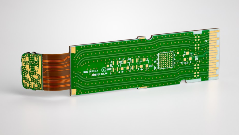
Gold fingers are the row of plated contacts along the edge of a board that plug into an edge connector or a card slot. They exist because the contact has to survive repeated insertion and removal without corroding, and gold over nickel is the combination that provides low and stable contact resistance at a modest normal force. The fingers are usually the only place on the board where electrolytic hard gold is used, because the plating has to be thick, dense and wear resistant, and because the fingers have to be connected to a common rail during plating, which is done through a plating bar that is cut off after the process.
The Plating Stack
The stack is copper, then a nickel barrier, then gold. The copper is the conductor and the base for the plating. The nickel layer, typically two to five micrometres, provides the hardness that supports the thin gold and acts as a diffusion barrier that stops the copper migrating into the gold. The gold, typically half a micrometre to one micrometre of hard gold, provides the corrosion resistance and the low contact resistance. Hard gold is an alloy with a small amount of cobalt or nickel, which raises its hardness and its wear resistance compared with pure soft gold; soft gold is used for wire bonding and for some connector applications but wears much faster on a sliding contact. A gold layer that is too thin wears through to the nickel in a few insertions, and one that sits on a poor or contaminated nickel layer will blister or flake rather than wear.
Finger Geometry
The fingers are defined by their length, width, pitch and position, and all four are set by the mating connector rather than by preference. The contact area is the part that actually touches the connector spring, and it should be a straight, clean rectangle with the plating extending beyond the contact zone at both ends so that wear is not concentrated at an edge. The pitch between fingers is limited by the connector and by the mask dam that has to survive between them. The fingers must be separated from the rest of the copper by a mask dam, and that dam determines the minimum pitch that can be produced reliably. Typically the plating is defined on the copper layer with a mask opening that is slightly larger, and the mask must not encroach on the contact area, because mask on a gold finger is both a cosmetic and a contact defect.
Bevel and Chamfer
The card edge is bevelled so that it enters the connector without catching, and the bevel is specified by an angle and a depth. Common bevel angles are between twenty and forty five degrees, with a depth that removes the corner of the board without reaching the plating. A bevel that cuts into the finger reduces the contact area and exposes the laminate; a bevel that is too shallow leaves a sharp edge that damages the connector or the inserter. Some designs use a double bevel for a symmetrical edge, and some require a specific radius at the finger tip to avoid stress concentration. The bevel is produced after plating and routing, so it must be specified as a separate operation with its own tolerance, and it is one of the operations that a supplier may or may not do in house, which affects lead time.
Plating Defects to Avoid
Thin gold. Shows as a short insertion life and, in the extreme, as porosity that allows the nickel to corrode.
Nickel contamination. A contaminated nickel bath produces a layer that the gold will not adhere to, so the plating blisters or peels under the contact force.
Plating bar remnants. The bar that carried the plating current has to be routed away cleanly; a stub of plated copper left on the edge is a shorting risk and an appearance defect.
Mask on the fingers. Produces an open contact and is usually caused by mask registration rather than by design intention.
Gold thickness variation along the finger. Caused by current distribution in the plating cell, and it matters because the thin end wears first.
Design and Cost Considerations
The plating thickness is the main cost driver, followed by the finger area and the number of boards in the plating batch. Thicker gold costs proportionally more because gold is expensive, and the plating bar and the bevel add operations. Where the connector is inserted only a few times in the life of the product, a thinner gold layer may be adequate, and where the product is repeatedly plugged and unplugged, the specification should follow the insertion cycle requirement rather than a default. It is also worth confirming that the gold fingers are the only use of electrolytic gold on the board, because adding a second gold plated area changes the plating connection scheme and can significantly complicate the process.

FAQ
How thick should gold fingers be? Commonly half a micrometre to one micrometre of hard gold over two to five micrometres of nickel. The right value depends on the number of insertion cycles the product will see.
What is hard gold? Gold alloyed with a small amount of cobalt or nickel, which raises the hardness and the wear resistance compared with pure soft gold.
Why is nickel used under the gold? It provides a hard support layer and a diffusion barrier that keeps copper from migrating into the gold.
What bevel angle is normal? Between twenty and forty five degrees, with a depth that removes the board corner without cutting into the plated contact area.
Can gold fingers be reworked? Only by replating, which is impractical. A finger that has been damaged by abrasion or contamination is normally a rejected board.
Conclusion
Gold fingers are a contact system, so they should be specified as a plating stack, a geometry and a bevel rather than as a feature on the edge of the board. Match the gold thickness to the insertion life, control the nickel so the gold adheres, keep the mask off the contact area, define the bevel and its tolerance, and confirm that the plating bar is routed away cleanly. The plating capability and the achievable tolerances are part of PCB capabilities, the finger and keepout geometry belongs in PCB design and layout, and the plating and bevel operations are described in PCB manufacturing. A prototype PCB assembly run with the real connector confirms the insertion before volume in 2026.